
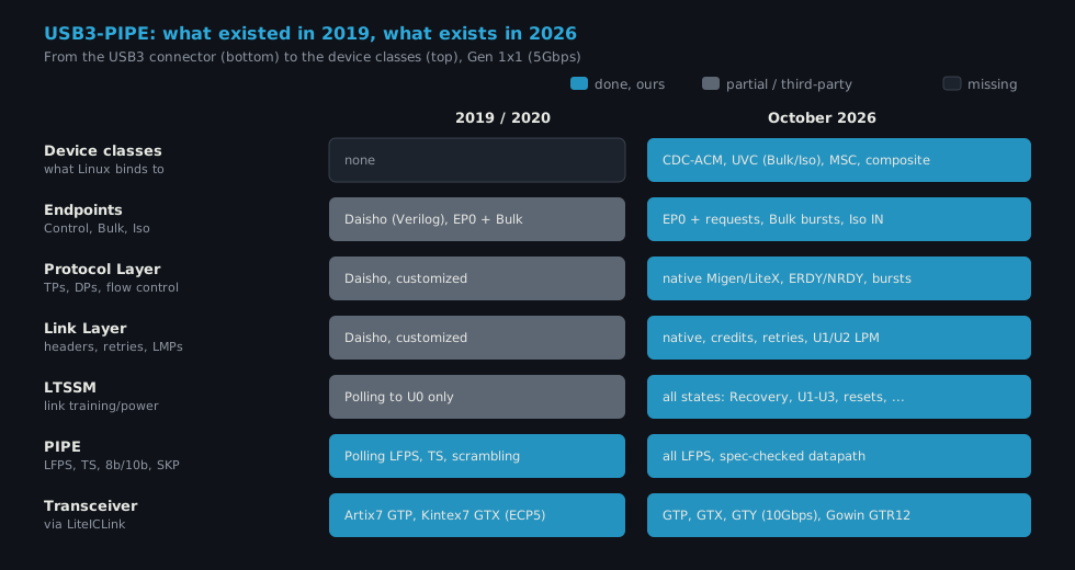
TL;DR: USB3-PIPE connects an FPGA transceiver straight to a USB 3 connector. The PHY layer, the link training state machine and the whole USB 3 device core run in the FPGA fabric, so no USB chip is needed. We started it in 2019 and brought the link up to U0, the state where data can flow, then stopped. Implementing the rest of the specification carefully enough for a real device was six months to a year of engineering. The initial funding covered a prototype and an experiment, not a full product development. This October, with agents in the loop, the parked project became a complete USB 3 device stack in Migen/LiteX. It runs Bulk transfers at 446/449 MB/s on an Acorn CLE-215+ (Artix7), with zero errors over 139 GB in full duplex, and it supports suspend/resume and standard Linux classes (serial port, camera, mass storage).
Why put USB 3 in the fabric#
An FPGA board that needs USB 3 usually gets a chip for it. The options are a USB 3 PHY such as the TI TUSB1310A, with a USB core still needed in the FPGA, or a complete controller such as the FTDI FT60x or the Cypress (now Infineon) FX3, seen by the FPGA as a FIFO or a parallel bus. Each one adds board area, cost, a vendor firmware or SDK, and a hard limit on what the device can be. Typical distributor prices in October 2026 (ballpark figures, they vary a lot with volume and stock):
| Chip | What it does | FPGA side | Unit price |
|---|---|---|---|
| Infineon (Cypress) FX3, CYUSB3014 | USB 3 controller with an ARM9 core, needs its own firmware, SPI flash and crystal | 32-bit GPIF parallel bus | about $20 in volume, $30 for one |
| FTDI FT601Q | USB 3 to 32-bit FIFO bridge | 32-bit synchronous FIFO | about $8 in volume, $10 for one |
| TI TUSB1310A | USB 3 PHY only, the USB core stays in the FPGA | PIPE parallel interface | about $6 to $18; TI lists it as not recommended for new designs |
For a board that already has a transceiver to spare, that is $6 to $30 per unit of BOM, plus the routing, the power rails and the vendor dependency. USB3-PIPE replaces all of it with logic.
Yet most mid-range FPGAs already have transceivers that run at 5Gbps and more: the GTP in an Artix7, the GTX in a Kintex7, the GTY in UltraScale+, and the GTR12 in the recent Gowin parts. A transceiver (also called a SerDes) serializes and deserializes the bit stream, and recovers the clock from the received data with its CDR (Clock and Data Recovery). USB 3 Gen 1 is a 5Gbps serial link with 8b/10b coding, like many protocols these transceivers are designed for. The idea of USB3-PIPE is to use the transceiver directly and do the rest in logic.
The name comes from PIPE, the PHY Interface for PCI Express, an Intel-defined interface between a USB 3/PCIe PHY and the controller above it. Discrete USB 3 PHYs expose PIPE. In USB3-PIPE the “PHY” behind that interface is built from a transceiver plus gateware.
2019: up to U0#
The project started in September 2019, with sponsoring from Google and Antmicro. Over the following weeks the pieces of the USB 3 physical layer came in one by one:
- LFPS (Low Frequency Periodic Signaling): bursts of a slow square wave sent while the link is electrically idle. This is how two USB 3 ports find each other and signal power state changes before any data symbols flow. On a transceiver, LFPS is generated by toggling the TX between a pattern and electrical idle, and detected from the RX idle detector.
- Training sequences: TSEQ, TS1 and TS2 ordered sets, used to train the receiver equalization, find the symbol alignment and agree on the link configuration.
- 8b/10b, scrambling and SKP: the data is scrambled to spread its spectrum, and SKP ordered sets are inserted and removed to absorb the frequency difference between the two ends. The host often uses SSC (spread spectrum clocking), sweeping its clock by up to 5000 ppm.
- The LTSSM (Link Training and Status State Machine): the state machine that sequences all of this, from Rx.Detect through the Polling substates to U0, the active state where packets can flow.
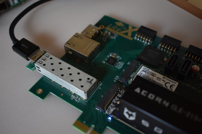
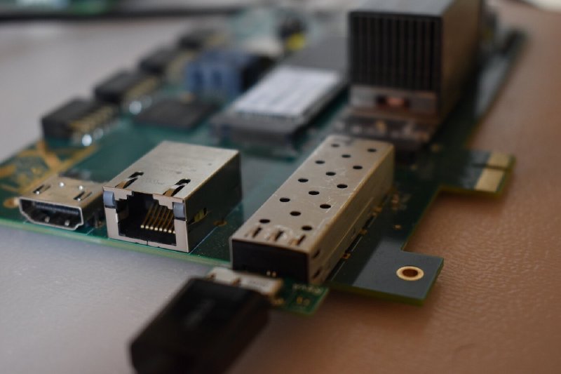
We tested on Kintex7 and Artix7 boards. bunnie designed a PCIsh-to-USB3.0 breakout board that plugged a USB 3 connector into a PCIe slot’s transceiver lanes. Later the SFP2USB adapter from the XillyUSB project did the same from an SFP cage, and that is what we still use.
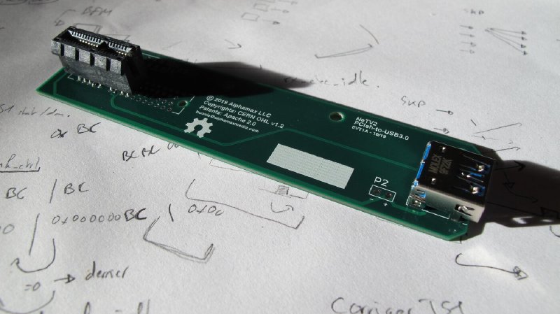
By December 2019 the link trained to U0 on hardware. For the layers above the PHY we integrated a customized version of the Daisho USB 3 core, a Verilog design originally written for a TUSB1310A PHY. With it, the board enumerated on some hosts, but not reliably, and that is where the project stayed for years.
Why it stopped#
Getting to U0 proved the concept. Turning that into a device someone can rely on means implementing the specification, not just the happy path. The USB 3.2 specification puts the physical layer and the link layer in chapters 6 and 7, and each of them is a long list of precise rules:
- every LTSSM state, with its entry conditions, exit conditions and timeouts: Recovery, the U1/U2/U3 low-power states and their exits, Hot Reset, Warm Reset, Compliance and Loopback;
- every kind of LFPS (Polling, Ping, U1/U2 exit, U3 wakeup, Warm Reset), each with its own timing windows;
- exactly how the scrambler advances, what happens to it around SKP and COM symbols, when SKP may be inserted;
- in the link layer, header sequence numbers, credits, retries, link management packets and their timers;
- in the protocol layer, flow control with NRDY/ERDY, bursts, short packets, and their interactions.
Any rule that is wrong or missing shows up on some host, at some point, as a link that drops into Recovery, a device that fails to resume, or an enumeration error. Debugging it on hardware without a USB 3 protocol analyzer is slow work: capture with LiteScope, compare against the spec, form a hypothesis, rebuild. We estimated it at six months to a year of focused engineering. The initial sponsoring had funded what it was meant to fund: a prototype showing that the idea works. Funding a full product development was a different matter, and for a small company it was not a reasonable investment on our own, so the project was parked.
What changed#
Agents change the cost of exactly this kind of work. A specification is a long list of rules that can each be checked. An agent can read a section, compare it with the code, write a test that exercises the rule, fix the gateware and move to the next one, and it does not get tired at rule number two hundred. What it cannot do alone is decide what matters, or see the hardware. Those two things drove how we set the work up.
After some groundwork at the end of 2025 (cleanup, CI, more tests), the real push came in October 2026, on these principles:
- The simulation comes first.
sim.pyconnects a host model and a device through two PHYs in Verilator, with clock offsets, SSC and word shifts. Every spec rule and every hardware finding becomes a test. The suite now has about 390 tests, plus long simulations marked as slow. - The hardware is observable from scripts. The PHY has debug CSRs that are always built in:
LTSSM state, the last 32 transitions with timestamps, and counters for every TS, LFPS and error
type. LiteScope groups capture the link, the datapath or the clock phase. The host side comes from
the kernel log.
bench/acorn_run.pyloads a bitstream, runs N link training attempts and records all of it, so an agent can run an experiment on the board and read the result. - One branch per topic. The repo history shows it:
fix/ltssm-exit-handshake,fix/lfps-warm-reset-detection,fix/rx-skp-remover-backpressure,fix/ts2-disable-scramblingand dozens more. Each branch is one section of the spec, checked, tested and merged on its own.
On 22 October the PIPE and LTSSM received about fifty spec fixes in one day. Examples: respond to an exit LFPS while it is being received; send LFPS as a real square wave; substitute every 8b/10b or disparity error with K28.4 as the spec requires; support the TS2 Disable Scrambling bit; honor Warm Reset in every state; and do the Idle Symbol handshake before U0. Some of them were subtle enough that they had never been visible on the 2019 setups. One example: the scrambler must advance per symbol, SKP symbols do not advance it, and a COM resets it in the middle of a 32-bit word. A word-level implementation works until a SKP lands at the wrong place.
A native device core in one day#
With the PHY solid, Daisho became the bottleneck. Its descriptors came back at the wrong offsets
(every descriptor request returned the Device Descriptor). Its string descriptors were generated
with wchar_t, which is 32-bit on Linux where USB expects UTF-16LE. And its structure was hard to
extend toward SuperSpeedPlus. On 23 October we wrote a native USB 3 Device Core in Migen/LiteX,
with Link Layer, Protocol Layer, control endpoint and Bulk endpoints, and tested it against a
scripted host model. That evening Daisho was removed from the repository.
The following days filled in what a device needs in practice:
- Bulk IN/OUT with bursts, and the NRDY/ERDY flow control with all its corner cases (stale ACKs, a window closed by a short packet, a pending ERDY cancelled by a new request).
- Isochronous IN endpoints, alternate settings, and U1/U2 link power management (
with_lpm). - Device classes that use the standard Linux drivers: CDC-ACM (a serial port, which can carry the LiteX BIOS console), UVC (a camera, up to 1080p60 over Bulk or 1080p30 isochronous), MSC (a mass storage RAM disk, or a DDR3 disk through LiteDRAM), and composite devices such as camera plus console.
- An EP0 Wishbone bridge, so
litex_server --usbcan reach the SoC bus over USB 3. - A Header Packets trace and a Link Layer events trace with timestamps, which show the protocol exchanges without a USB analyzer.
- A standalone Verilog generator (
usb3_pipe_gen) for projects that do not use LiteX.
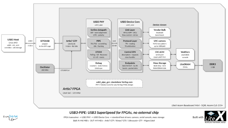
All of this costs little logic on a mid-range FPGA. Measured with Vivado 2024.1 on the Acorn’s XC7A200T (133,800 LUTs), timing met at 125 MHz:
| LUTs | Flip-flops | Block RAM (36Kb) | Share of an XC7A200T | |
|---|---|---|---|---|
| Device core alone (Link + Protocol Layers, EP0, Bulk IN/OUT) | 2,550 | 1,682 | 4 | 1.9% |
| Complete Bulk loopback design (transceiver, PHY, core, debug CSRs, traces, UART bridge) | 8,716 | 5,094 | 5 | 6.5% |
The complete design includes about 2,800 LUTs used as distributed RAM (FIFOs and traces) and the debug logic we keep in every bench build. On an XC7A100T it would still use less than 14% of the LUTs, which leaves most of the FPGA for the application, and replaces a $6 to $30 chip.
The Acorn and its GTP#
The Acorn CLE-215+ was built as a cryptocurrency mining accelerator: an Artix7 XC7A200T on an M.2 card. It is now cheap on the second-hand market. On the LiteX Acorn Baseboard it gets an SFP cage, Ethernet and SATA. It is our main 5Gbps target, and it found three hardware issues that no simulation would have shown.
The reference clock. The Acorn has no transceiver reference clock without a PCIe host: the GTP’s dedicated clock input comes from the PCIe edge connector, and we measured 0 Hz there on the baseboard. The 200 MHz oscillator therefore comes from the fabric. When it reached the GTP through the GTREFCLK0 input, the clock went through general interconnect. The RX quality then depended on the place and route: some bitstreams kept a clean link, others never reached a stable U0. Timing slack, fabric load and nearby logic made no difference. Routing it to GTGREFCLK0, an input UG482 reserves for internal testing but the only one that uses the clock network, gave stable links on 13 of 13 builds, against 0 of 9 for the bad GTREFCLK0 builds. This is now an option in LiteICLink (#55).
An RX stuck in 16-bit mode. The GTP RX initialization works around a silicon issue: it clears
a bit of the RX data width attribute (DRP address 0x011) during the PMA reset, then restores it.
If an RX re-initialization restarted between those two steps, the “restored” value was the
modified one. The RX then stayed in 16-bit mode, at 312.5 MHz instead of 250 MHz, and link training
failed. From the outside this looked like a marginal receiver that depended on the build and on
luck. The fix is in LiteICLink
(#54), and usb3_debug.py rx-check now
checks every bitstream for it.
Suspend and resume. Linux autosuspends idle devices with a driver: the link goes to U3, and the device resumes when it is used again. About half of our resumes failed and fell back to a host reset. Several fixes that looked plausible changed nothing: re-initializing the RX, CDR settings, longer LFPS. The captures that explained it started from the end of our wakeup LFPS. The host’s TS1 and TS2 ordered sets were decoded with the CDR locked, but the GTP comma aligner slid on every ordered set, about 1100 realignments in 32 µs. It was set to align commas on even bytes only, which conflicts with the consecutive COM symbols of USB 3 ordered sets whenever the first one arrives on an odd byte. After U3 that is random. Aligning on any byte, and letting our word aligner handle the rotation, gave 72 clean resumes out of 72, in about 0.6 s each.
Results#
All the numbers are measured on the Acorn with a Linux xHCI host and the standard drivers:
| Acorn CLE-215+, Artix7 GTP, Gen 1x1 (5Gbps) | |
|---|---|
| Enumeration | SuperSpeed (5000M) |
| Bulk IN / OUT | 446 / 449 MB/s, about 90% of the 500 MB/s that 5Gbps carries after 8b/10b |
| Full duplex | 376 + 400 MB/s |
| Stability | 139 GB in full duplex, data checked: 0 errors, no retry, no Recovery |
| Suspend/resume | Linux autosuspend (U3) and resume: 72/72 clean, about 0.6 s |
| Demos | Bulk loopback/bench, LiteX BIOS console over CDC-ACM, UVC camera, MSC disk, composite |
The same design also builds for the KC705 (Kintex7 GTX), where hardware validation is still in progress. From there, the next step was 10Gbps: SuperSpeedPlus on a Kintex UltraScale+, and then the port to Gowin FPGAs.
Try it#
git clone https://github.com/enjoy-digital/usb3_pipe && cd usb3_pipe
pip3 install -e .

# Simulation: host model <-> PHYs <-> device core (link training, enumeration, Bulk).
./sim.py
pytest test

# Acorn + SFP2USB: build, load, check the enumeration, run a loopback.
./bench/acorn.py --build --load --with-jtagbone
lsusb -t
./bench/usb3_bulk.py loopback --size 1024 --count 1000

# Other examples: --example bench|console|uvc|uvc_iso|msc|msc_dram|composite|wishbone
./bench/acorn.py --build --load --example uvc
ffplay -f v4l2 -video_size 1920x1080 /dev/video0
The debugging guide describes the hardware flow, from the CSR counters to the LiteScope captures.
Thanks to bunnie for the PCIsh-to-USB3.0 breakout board, to Antmicro and Google for sponsoring the initial development, to the Daisho project whose core carried the first enumerations, and to Xillybus for the SFP2USB adapter.
Work and ideas by Enjoy-Digital; written up with AI in the loop.