
TL;DR: USB3-PIPE is a USB 3 device built in the FPGA fabric. It runs at 5Gbps on an Artix7 and at 10Gbps on a Kintex UltraScale+. Gowin’s GW5A family has transceivers that can do USB 3, but its fabric is about twice as slow per logic level, and the vendor tools have less margin to give. To make it fit, the PIPE stays at the line rate in its own clock domain, and everything above it runs at half the frequency on 64-bit words. We also dropped the U1/U2 power states and reworked the datapaths. The Sipeed Tang Mega 138K Pro now runs Bulk transfers at 372/433 MB/s with zero errors. The same stack then went into a much smaller part, the GW5AT-15 of Sipeed’s SLogic16U3 USB 3 logic analyzer, where it enumerates at 5Gbps and streams captures at 400 MB/s, the analyzer’s full rate.
What Xilinx gave us for free#
The first two steps of this work ran on Xilinx devices, and in hindsight that made them easier than they looked.
On the Acorn’s Artix7, the whole stack above the transceiver runs in one 125 MHz clock domain on 32-bit words, with margin to spare. On the XCKU3P’s UltraScale+, the Gen 2 datapath runs at 250 MHz on 40-bit words, and the 64-bit link layer was a refactoring rather than a timing project. Most of the USB3-PIPE logic is not careful about logic depth: FSMs with many conditions, wide multiplexers and comparisons computed directly from registers. On these fabrics, it simply met timing.
Vivado deserves a lot of the credit. Its synthesis infers what you meant, its placer and router are timing-driven and robust, and its reports show exactly where the problem is when there is one. When timing fails, the question is almost always our design, not the tool’s output. Vivado is a marvel of engineering, the result of decades of work and probably billions invested by Xilinx (now AMD) in its devices and tools. Developers like to complain about it, and we have done our share; spending a few days with another vendor’s tools is a good way to remember how much it does for you.
The Gowin GW5A#
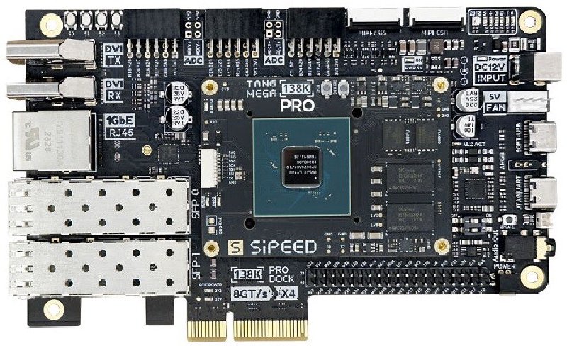
Gowin’s Arora V family (GW5A) is a big step for Gowin: up to 138K LUTs, hard PCIe and the GTR12 transceivers, which reach 12.5Gbps. The parts are inexpensive, and boards such as Sipeed’s are widely available. We already support several GW5A boards in LiteX.
The first USB3-PIPE builds for the GW5AST-138B, on the Sipeed Tang Mega 138K Pro, showed the gap. Each logic level costs roughly twice what it costs on an Artix7, and the paths are dominated by routing: about 1.3 ns per hop, two thirds of the total delay. A design that has a few levels too many on Xilinx misses on Gowin by a wide margin.
The tools add their own constraints:
- Synthesis: GowinSynthesis merged the block ROMs it inferred from the 8b/10b decoder and checker lookups, which share an address, into one ROM with the wrong contents. On hardware, no COM symbol was ever decoded. Initialized asynchronous-read memories were not kept either. On the SLogic16U3, a small FIFO with an asynchronous read was implemented in block RAM, which cannot do that: control requests read back as zeros. Each case was fixed in our code (lookups forced into logic, ordered sets as constants, a buffered FIFO). We also added a build check that rejects asynchronous reads left to the Gowin memory mapping.
- Place and route: the placer has no seed, so the only way to explore is to try its different
place algorithms. The results vary by about ±15% between runs. On the larger Gen 2 builds, the
timing-driven router left nets unrouted, so we use the non-timing-driven one.
build_best.pybuilds the place algorithms in parallel and keeps the one with the best margins.
None of this makes the GW5A a bad target. It means the design has to be written for it.
What we cut, and how we split it#
Getting 5Gbps on the Tang meant deciding what had to run fast and what did not.
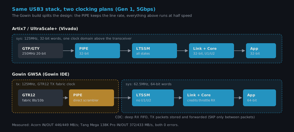
Two clock domains. The PIPE has to process the line rate: at 5Gbps that is 500 million symbols
per second, which means 32-bit words at 125 MHz with no way around it. Everything above it, from the
LTSSM to the link layer, the device core and the application, can run at half the frequency on
words twice as wide. USB3PHY(pipe_cd=...) puts the PIPE in its own domain on the GTR12 TX clock
at 125 MHz. The LTSSM, link layer and core run at 62.5 MHz on 64-bit words, the format the Gen 2
work had already introduced.
The split has consequences that the single-domain design never had to handle:
- CDC (clock domain crossing): LTSSM requests and PIPE events cross between the two domains, both as levels and as pulses. Training sequences are now always completed on an ordered set boundary, because a request can arrive at any point of a word.
- RX flow control: Bulk OUT data arrives at line rate, faster than the slower side can always accept it. A deep RX FIFO absorbs bursts, and the link layer holds back its receive credits while the FIFO is half full, so the host waits instead of overflowing it.
- TX framing: packets are stored and forwarded, and SKP ordered sets are only inserted between packets. The Linux host rejected header packets with a SKP inside them on this target.
Less depth everywhere. The PIPE logic was rewritten for fewer levels per path without changing its behavior. The scrambler computes each symbol’s LFSR state directly from the current state instead of chaining symbol after symbol. The TS checkers have registered inputs and outputs. The async FIFOs have a registered read, and registered skid buffers surround the CDC FIFOs. These changes are generic and benefit the Xilinx targets too.
Features a device can live without. The LTSSM is built with with_u1u2=False on Gowin: U1 and
U2, the two light low-power states, are rejected. The host falls back cleanly, U3 suspend/resume is
kept, and the logic and its timing paths go away. On the small part, the device core only gets the
endpoints the application uses.
The transceiver side needed new support too. LiteICLink gained the GTR12
(#57, raw PCS with 8b/10b in the fabric,
then #58 for runtime register access and
wider raw words). The GTR12 configuration registers are generated with Gowin’s serdes_toml_to_csr
from Sipeed’s PHY configuration.
Tang Mega 138K Pro: 5Gbps#
With these changes the Tang build met timing on all clocks: TX at 125.1 MHz, RX at 141.0 MHz and sys at 63.9 MHz, against 125/62.5 MHz required. The margins are thin, but they are real. On hardware, with a Linux xHCI host:
| Tang Mega 138K Pro, GW5AST-138B GTR12, Gen 1x1 (5Gbps) | |
|---|---|
| Enumeration | SuperSpeed (5000M) |
| Bulk IN / OUT | 372 / 433 MB/s (64-bit link layer at 62.5 MHz) |
| Full duplex | 262 + 383 MB/s |
| Stability | 20 s runs, data checked: 0 errors, 0 LBAD, 0 Recovery |
That is below the Acorn’s 446/449 MB/s. Bulk IN in particular pays for the slower side’s reaction time. It is a complete, standard USB 3 device on a Gowin FPGA, with no USB chip and no vendor USB IP, and this support is now merged (USB3-PIPE #153).
On the GW5AST-138B the cost stays small, even with the wider 64-bit datapaths and the extra buffering the split requires. Measured with Gowin 1.9.12 (Bulk loopback design with the debug CSRs and the UART bridge, timing met: tx 130 MHz, rx 145 MHz, sys 69 MHz):
| Logic (LUT + ALU) | Registers | Block RAM | Share of the GW5AST-138B | |
|---|---|---|---|---|
| Complete design (GTR12, PHY, core, debug) | 10,548 | 6,069 | 46 BSRAM | 8% logic, 5% registers, 14% block RAM |
SLogic16U3: USB 3 in 15K LUTs#
The Tang has 138K LUTs to spare. The SLogic16U3 is a Sipeed USB 3 logic analyzer built around a GW5AT-15, a 15K LUT part. As on the Tang, its GTR12 transceiver goes straight to the USB-C connector, with only a Type-C lane mux in between. The analyzer sells for about $60 to $70. An FX3 alone would cost $20 to $30 of that: at this price point, using the FPGA’s transceiver for USB 3 makes a real difference. We are writing open LiteX gateware and a host stack for it; here we only look at the USB 3 part.
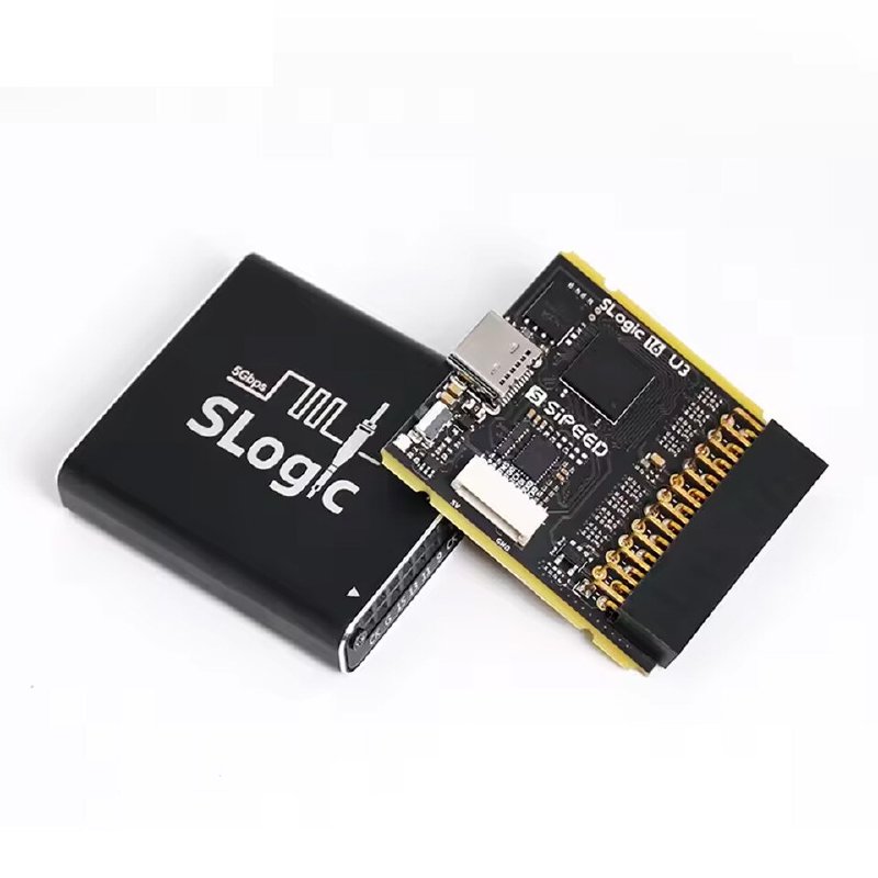
The cuts mattered even more here. The USB 3 PHY and device core take about 10.4K logic cells, about the same as on the Tang. That was 8% of the GW5AST-138B, but it is 69% of the GW5AT-15, and the complete design fills 88% of the logic. With Gowin IDE 1.9.12.04 it meets timing: 74.7 MHz for the 62.5 MHz side, 131.5 MHz for the 125 MHz PIPE.
The Gowin version matters on this part. With 1.9.10, only one of the five place algorithms met
timing; with 1.9.12, four of them do. The transceiver configuration also needs 1.9.12: its
GW5AT-15 specific serdes_toml_to_csr produces the registers that match Gowin’s USB 3.0 PHY IP
configuration, while the generic 1.9.10 tool missed some of them and wrote registers for a second
quad that this device does not have. The hardware bring-up found the rest:
- with the GTR12’s QPLL1, the host never saw a device. QPLL0, the PLL that Gowin’s own USB 3.0 PHY IP configuration selects on this part, works;
- the CDR value generated from the TOML gave 8b/10b errors and Polling.Idle timeouts. The value from Gowin’s USB 3.0 PHY IP configuration trains cleanly;
- the asynchronous-read FIFO mapped to block RAM, described above, made every control request read back as zeros.
One more finding was on the USB side: Bulk IN first stalled around 370 MB/s, with the device waiting for a host request about half of the time. The AMD xHCI host counts its requests down from the endpoint’s Max Burst, and with a Max Burst of 8 it asks for more data too late. With a Max Burst of 16 and more buffering, the SLogic16U3 enumerates at 5000M and sustains 400 MB/s of Bulk IN, the analyzer’s full rate.
10Gbps on Gowin#
The GTR12 can run at 10Gbps, and the Gen 2 work is ready to use it. Switching the GTR12 from 5 to 10Gbps takes six register writes at runtime, with the same 5 GHz VCO and fabric clock. The raw words grow from 40 to 80 bits. The Gen 2 framing now processes 16 bytes per cycle. The block aligner, gearbox and DC balance were restructured for few levels and low fanout: a one-hot block aligner pointer, decodes registered and shifted with the data window, data registers without reset. The first Gen 2 Tang builds ran at 41 MHz for the transceiver clocks. Today’s build closes timing at 125/62.5 MHz. The 10Gbps bring-up on the Tang is next (USB3-PIPE #154).
Try it#
# USB3-PIPE on the Tang Mega 138K Pro (Gowin IDE, LiteICLink with GTR12 support).
git clone https://github.com/enjoy-digital/usb3_pipe && cd usb3_pipe
pip3 install -e .
./bench/sipeed_tang_mega_138k_pro.py --build --example bench
openFPGALoader -c ft2232 build/sipeed_tang_mega_138k_pro/gateware/impl/pnr/project.fs
./bench/usb3_bench.py both --transfer-size 65536 --csr-csv build/sipeed_tang_mega_138k_pro/csr.csv

# Simulation of the split clocking (PIPE in its own domain, no U1/U2).
./sim.py --dev-pipe-cd --dev-no-u1u2
Thanks to Sipeed for the hardware, the DFU loader and the board photo. The slogic16u3-trace project documented the SLogic16U3 pinout, DFU protocol and flash layout. Kenta Ida wrote the first open USB 3 stack on the SLogic16U3.
Work and ideas by Enjoy-Digital; written up with AI in the loop.