
TL;DR: USB3-PIPE started as a USB 3 Gen 1 (5Gbps) device in the FPGA fabric, running on an Artix7. Gen 2 (10Gbps, called SuperSpeedPlus) is a different physical layer: 128b/132b blocks instead of 8b/10b, a new scrambler, a speed negotiation, and a link layer with new flow control rules. We wrote and checked all of it in simulation first, against the specification’s own figures and tables, since our 5Gbps board could not run at 10Gbps. Then we moved to a second-hand Alibaba Cloud XCKU3P card (Kintex UltraScale+, about $100) with an SFP2USB adapter. It enumerated at 10000M and passed Bulk transfers after about a day and a half of bring-up. It now reaches 785 MB/s IN and 881 MB/s OUT, with zero errors over 120 s full duplex soaks.
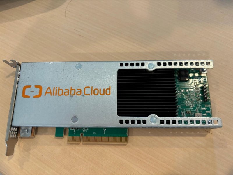
The card#
This board was a datacenter NIC accelerator for Alibaba Cloud. It now sells second hand for roughly $60 to $120: a Kintex UltraScale+ XCKU3P, PCIe Gen3, two SFP28 cages wired to GTY transceivers, and a 156.25 MHz reference clock for those cages. The XCKU3P is covered by Vivado’s free license. We added it to LiteX-Boards at the end of 2025 (#715) and already use it as a multi-rate Ethernet NIC.
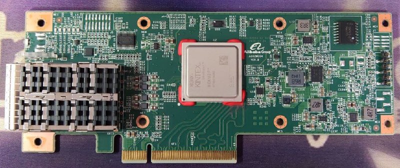
For USB 3, the useful part is the SFP cages. The same SFP2USB adapter that serves the Acorn fits there, and the GTY transceivers go well beyond 10Gbps. The Artix7 GTP on the Acorn stops at 6.6Gbps, so it cannot do Gen 2 at all.
Before Gen 2, the card had to run Gen 1. That needed a GTY version of the USB3-PIPE SerDes
(USPUSB3SerDes) and the GTY reference clock taken from the SFP cages’ 156.25 MHz clock. Gen 1
then ran with the shared example designs: 446 MB/s IN and 450 MB/s OUT, the same
as on the Acorn.
What Gen 2 changes#
Moving from Gen 1 to Gen 2 is not a clock change. Most of the physical layer is new:
- 128b/132b coding. Gen 1 uses 8b/10b, where every byte becomes a 10-bit symbol (20% overhead). Gen 2 sends 132-bit blocks: a 4-bit block header that says whether the block holds data or control, then 128 bits of payload (3% overhead). The receiver has to find the block boundaries in the raw bit stream itself. This “block aligner” searches for the header pattern and locks on special SYNC ordered sets. The transceivers’ built-in 64b/66b gearbox does not fit this format, so a fabric gearbox converts between blocks and 40-bit transceiver words.
- A new scrambler, a 23-bit LFSR with different rules for what is scrambled, what advances it and what resets it. There are also new ordered sets (SYNC, SDS for start of data stream, variable-length SKP) and DC balance symbols computed by the transmitter.
- Speed negotiation. Before training, a SuperSpeedPlus port has to find out what its partner supports. It does this with LFPS again: SCD1/SCD2 patterns, then LBPM (LFPS Based PWM Messaging), which encodes bits in the duty cycle of the LFPS bursts. The two ports exchange their PHY capabilities, agree on the highest common mode, and only then switch their transceivers to 10Gbps.
- The SuperSpeedPlus link layer: 4-bit header sequence numbers instead of 3, two traffic classes (Type 1 for headers, Type 2 for data headers) with separate buffers and separate credits, nullified data payloads after a retransmission, and different timer values.
The protocol layer, the endpoints and the device classes stay almost the same, and that is where most of the work of the Gen 1 core lives.
Simulation first#
The Acorn could not run any of this, and the XCKU3P was still being brought up at Gen 1, so every Gen 2 block was written against the specification and tested in simulation. The tests are unusually literal:
- the scrambler test re-implements Figure 6-12 of the USB 3.2 specification register by register and compares the two;
- the transmitter output is decoded by an independent bit-serial reference model of the specification’s rules: TS contents, DC balance symbols, the LFSR values carried in the SKP ordered sets, SKP and SYNC scheduling;
- the receiver is fed through a channel model that inserts bit offsets, polarity inversion, bit slips during training, block header bit errors, and SKP ordered sets shortened or lengthened.
On the protocol side, sim.py --gen2 trains a host model and a device to U0 at Gen 2 in Verilator.
The SuperSpeedPlus negotiation is tested against Gen 2 hosts, Gen 1 hosts and dual-lane hosts. Some
details stayed marked as “approximated / not verified” in the roadmap until a real host could
settle them: the bit order of the block header, the LBPM capability bits, and the moment of the
speed switch.
Four milestones on hardware#
The bring-up followed milestones, each with its own CSRs and snapshots, so we could see how far the link got before trying the next step.
M1, Gen 2 capability and RX. The device advertises Gen 2 during the SuperSpeedPlus Polling, the host selects it, and the GTY switches to 10Gbps. The goal was to receive and decode the host’s ordered sets correctly before transmitting anything meaningful: 31.6 million blocks were aligned and descrambled, and the bit order and the SKP LFSR symbols matched the simulation. Two issues only showed up on hardware:
- A
popcountcompared to constants was evaluated on 1-bit operands in the generated Verilog. Every block header then looked like a corrected control header. The Migen simulation computed it correctly, so it was invisible there. It is now fixed and tested with Yosys on the generated Verilog. - The GTY CDR settings from the Transceivers Wizard default for 10Gbps did not track the host’s spread spectrum clock. The settings we already used at 5Gbps (close to the PCIe Gen3 ones) did.
M2, link training to U0. The Gen 2 PIPE runs under the LTSSM once Gen 2 is negotiated: Polling.RxEQ (524,288 TSEQ, 6.9 ms), Polling.Active, Polling.Configuration, Polling.Idle, then U0 at 10Gbps. A detail the simulation had wrong: the Gen 2 Idle Symbol is 5Ah. We found it by descrambling the host’s data blocks after SDS. At this point the Gen 1 link layer received nothing and the link fell into Recovery a few microseconds after U0, which was expected: the next layer was missing.
M3, SuperSpeedPlus link layer, enumeration and Bulk. The Gen 2 packet framing (link layer words
to and from data blocks) and the SuperSpeedPlus link layer went in, with the SuperSpeedPlus
capability added to the BOS descriptor. lsusb -t showed 10000M. The first Bulk numbers were
320 MB/s IN and 466 MB/s OUT, with no errors and no Recovery. Full duplex was weak, at 98 + 457
MB/s. Fixes from this step: Warm Reset detection could not use 8b/10b errors at 10Gbps (raw words
always look invalid as 8b/10b), so it now uses the loss of block alignment. The PENDING_HP_TIMER
is 10 µs (Table 7-7). A burst of packets packed back to back could starve SKP ordered sets, which
made the host enter Recovery every few milliseconds in full duplex.
M4, throughput and robustness. A throughput profile in the bench design measures where the link layer and the Bulk IN endpoint spend their cycles. It showed the next fixes:
- separate Type 1 and Type 2 header buffers, so Bulk OUT ACKs no longer block Bulk IN data headers;
- LGOOD/LCRD link commands taken out of the RX framing without waiting behind the RX data;
- a rare packer bug that inserted an idle block inside a packet.
Full duplex went from 100 + 457 to 325 + 430 MB/s. At that point the limit was the 32-bit link
layer itself, about 470 MB/s at 125 MHz, so the last step widened it to 64 bits (link_words=2),
including the DPP datapath, the CRC-32 on 8 bytes and the Bulk endpoints. Robustness tests covered
retraining after PHY resets, alternating Gen 2 and Gen 1, and U1/U2 at Gen 2 in simulation.
From the first Gen 1 link on the XCKU3P (27 October, late morning) to the 64-bit Gen 2 results (28 October, late afternoon) took about a day and a half.
Results#
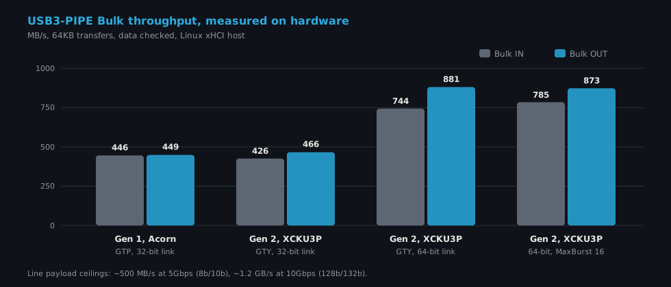
| XCKU3P, Gen 2x1 (10Gbps), 64KB transfers | Bulk IN | Bulk OUT | Full duplex (IN + OUT) |
|---|---|---|---|
| 32-bit link layer | 426 MB/s | 466 MB/s | 325 + 430 MB/s |
| 64-bit link layer | 744 MB/s | 881 MB/s | 619 + 736 MB/s (120 s soak) |
| 64-bit, MaxBurst 16 | 785 MB/s | 873 MB/s | 644 + 757 MB/s |
All runs check the data: 0 errors, 0 LBAD (link layer bad packets), 0 Recovery over 156 GB in full duplex. The same Gen 2 capable design falls back to Gen 1 on a Gen 1 host, at 441 MB/s.
The Gen 2 design is larger, mostly because of the 128b/132b datapaths at 250 MHz, the 64-bit link layer and the Gen 2 bring-up instrumentation, but it stays small on this FPGA. Measured with Vivado 2024.1 on the XCKU3P (162,720 LUTs), Gen 2 capable Bulk loopback design with the 64-bit link layer, timing met:
| LUTs | Flip-flops | Block RAM (36Kb) | Share of the XCKU3P | |
|---|---|---|---|---|
| Complete design (GTY, Gen 1 + Gen 2 PHY, 64-bit core, Gen 2 debug snapshots and counters, JTAG bridge) | 20,042 | 13,551 | 18 | 12.3% LUTs, 4.2% flip-flops, 5% block RAM |
Most of the Gen 2 debug logic (raw word snapshots, block snapshots, link command counters) can be removed once the bring-up is over.
Two limits remain. Bulk OUT uses about 87% of what 64-bit words at 125 MHz can carry (1 GB/s), against about 1.18 GB/s on the line. Bulk IN waits on the host’s requests. One measurement detail: with 1 MB transfers, the host itself limits Bulk IN to about 330 MB/s, so the device numbers use 64 KB transfers.
What is next#
The Gen 2 work also made the stack more general. The Gen 2 framing, the 64-bit link layer and the pipelined datapaths are what made the Gowin port possible. The next steps on Xilinx devices:
- the last ~25% of Gen 2 Bulk OUT (wider or faster link layer words), and 64-bit datapaths for the camera and mass storage classes;
- Gen 2 SerDes clocking for the Kintex7 GTX and UltraScale GTH, which can also reach 10Gbps;
- Gen 1x2 (two 5Gbps lanes over USB-C): the PHY with lane striping and deskew is done in simulation. The hardware needs a USB-C breakout with both SuperSpeed pairs routed to transceivers, plus CC handling;
- Gen 2x2 (20Gbps), the combination of both, on the UltraScale+ GTY.
Try it#
git clone https://github.com/enjoy-digital/usb3_pipe && cd usb3_pipe
pip3 install -e .

# Gen 2 in simulation: host and device to U0 at 10Gbps, enumeration, Bulk.
./sim.py --gen2

# XCKU3P + SFP2USB in the NIC1 cage, on a USB 3.2 Gen 2 host port.
./bench/alibaba_xcku3p.py --build --load --example bench --gen2-capable --link-words 2
lsusb -t                                   # 10000M
./bench/usb3_bench.py both --transfer-size 65536 --csr-csv build/alibaba_xcku3p/csr.csv
The Gen 2 roadmap covers each milestone in detail, including what is still approximated.
The GTY raw symbol and rate controls went into LiteICLink (#56). Thanks to TiferKing for the board photo and the AS02MC04 board files, and to essenceia for the photo of the card in its shroud.
Work and ideas by Enjoy-Digital; written up with AI in the loop.