
TL;DR: TriXium runs PrismML’s ternary Bonsai language models entirely on an FPGA card: the host only tokenizes, and every weight of the model is streamed from the card’s memory for each token. It is a project we had wanted to do for a long time, because it is the perfect stress test for the LiteX ecosystem: LitePCIe to talk to the host, LiteDRAM (and HBM2) to feed the engine, and a design whose speed is set almost entirely by how many bytes per second the memory delivers. We started on two large second-hand cards, an FK33 with 8 GB of HBM2 and an XCU1525 with four DDR4 controllers, to get everything in place with plenty of FPGA margin, and pushed them to 106 tok/s on the 1.7B model and 30 tok/s on the 8B. The fixes went back into LiteX and LiteDRAM along the way. Then we finished LiteDRAM’s support for an inexpensive Inspur Kintex-7 card, the YPCB-00338, packed the design into it, and got 35 tok/s on the 1.7B and 8 tok/s on the 8B from two DDR3 channels, on the same card that openTPU uses.
Why ternary, and why it is a memory problem#
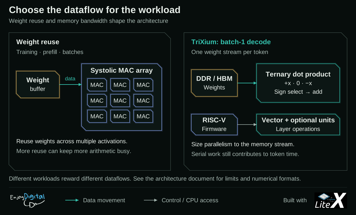
When one user chats with a language model, the model generates one token at a time, and each token runs every layer once. Nothing is batched, so every weight is read from memory once per token and used once. This is called batch-1 decode, and its speed limit is simple: the bytes of the weights divided by the memory bandwidth. The arithmetic hardly matters; a large multiplier array would mostly wait for memory.
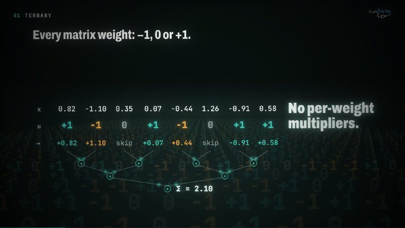
PrismML’s Bonsai models make the bytes small. Every matrix weight is -1, 0 or +1 (a trit), plus one fp16 scale shared by each group of 128 weights. Stored as 2 bits per trit, that is 2.125 bits per weight, about 4x fewer bytes than int8. And the arithmetic becomes trivial: multiplying an activation by a trit is selecting +x, nothing, or -x. A group of 128 weights is an adder tree, then one multiply by the group’s scale.
So TriXium is not a TPU. A systolic array of multipliers is built to reuse each weight many times, which batch-1 decode never does. TriXium’s engine is adder trees sized to exactly the bytes the memory can deliver, and the rest of a layer (norms, attention, SiLU, the KV cache) runs on a VexiiRiscv RISC-V CPU running C, a small microcoded vector unit, and fixed-function units added only where profiling showed they pay. Each bitstream is specialised at build time for a board and a model family, like a hand-written GPU kernel: no logic is spent on flexibility the model never uses.
Start big, with margin#
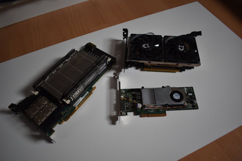
Building on the smallest possible FPGA from day one would have mixed two problems: making the design correct and fast, and making it fit. So we started on the largest cards we could get, both retired cryptocurrency-mining accelerators that now sell second-hand:
- the SQRL FK33 (Virtex UltraScale+ VU33P) with 8 GB of HBM2 in the package, two stacks and 32 pseudo-channels;
- the SQRL XCU1525 (Virtex UltraScale+ VU9P, a VCU1525 clone) with four DDR4 DIMMs on four independent 64-bit channels.
The design is one LiteX SoC per board. A target file supplies the clocks, the CPU, LitePCIe and the memory system, and instantiates one TriXium core with three standard interfaces: one 256-bit AXI master per engine channel, a Wishbone slave for the CPU, and a stream for the weight upload. The same core then runs on HBM2, DDR4, DDR3, and in Verilator.
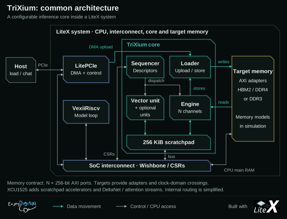
Each matrix is split row-wise across the engine channels, so every channel streams its own slice of the weights in parallel from its own memory window. The CPU runs the model loop and posts pre-built descriptor lists to a sequencer, which dispatches them back to back to the engine and the units. On the FK33, the 16 channels map onto 16 HBM2 pseudo-channels; on the XCU1525, onto four LiteDRAM DDR4 controllers, four channels each.
Correctness came first, and it was designed in rather than tested afterwards. A Python mirror reproduces the firmware’s arithmetic bit for bit, including the CPU’s own float paths, and the whole SoC runs in Verilator with the real firmware on a tiny model with the target’s structure: 87 FP32 checkpoints compared against the mirror, bit-identical. A unit only landed once it reproduced the CPU path exactly, and every board run checks the first tokens against the reference before reporting a speed. A fast wrong answer is not a result.
The climb on the FK33#
The first tokens came on 4 August, eight days after the first commit: the 1.7B model answered " Paris" on the card at 2.03 tok/s. Five weeks later, on the same card, it ran at 101.9 tok/s, and the shipping build reaches 106.3.
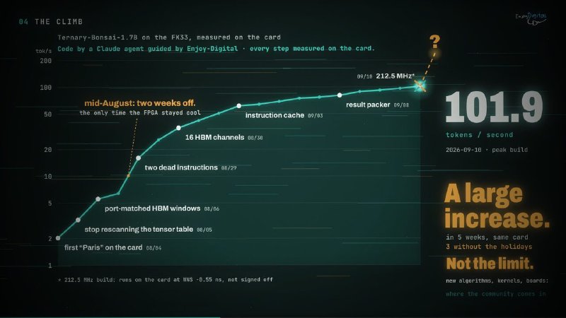
Almost none of it came from the engine’s raw width. The steps that mattered:
- HBM addressing. A matvec ran at ~4.6 cycles per beat. The cause was not the reads but the layout: channel c’s weights were read across the HBM’s internal switch instead of from its own pseudo-channel. Port-matched windows took it to 1.48 cycles per beat.
- The soft CPU. A per-cycle profiler showed half of the CPU’s cycles retiring nothing: 63 KB of hot firmware through a 4 KB instruction cache backed by HBM. Replacing VexRiscv by VexiiRiscv (bigger caches, branch prediction) took a token from 31.2 M to 13.8 M cycles.
- A pipelined vector unit, sixteen channels, then 32 KB caches: 25 to 75 tok/s.
- Every write counts. The vector unit ran 2.9x slower under an engine stream, because every matvec result was its own scratchpad write. Packing eight results per write took the card to 80.6 tok/s.
- Timing. A 225 MHz campaign hit routing congestion, not logic depth. 212.5 MHz worked.
Once there, the FK33 is engine-bound rather than memory-bound: the 8B moves about 61 GB/s at 30.3 tok/s, far from what the HBM2 can deliver. For a card that sells second-hand for a few hundred dollars, it runs level with an Apple M4 Pro’s CPU on the same models (106 against 123 tok/s on the 1.7B, 30.3 against 32 on the 8B, using PrismML’s published figures).
The XCU1525, and making LiteDRAM fast enough#
The XCU1525 is the opposite case: no HBM, four DDR4 channels driven by four LiteDRAM controllers, 48 GB/s in total. Here the engine is cheap and the memory is the wall, so this is where LiteDRAM itself had to get faster.
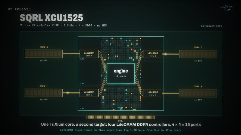
The first XCU1525 tokens, on 19 September, ran the 1.7B at 5.56 tok/s, against 101 on the FK33. The cause was in LiteDRAM: its native-port up-converter, which turns narrow port accesses into the controller’s wide words, allowed only one read in flight. Pipelining its reads (LiteDRAM #413) took the 1.7B to 49.6 tok/s, and it helps any LiteDRAM design that streams reads through a narrower port.
DDR4 calibration was the second problem. LiteX’s liblitedram calibrates by reading back what it wrote, so it cannot tell a wrong read delay from a wrong write delay, and some byte lanes came out of write leveling at the edge of their eye. DDR4 has a better tool for this: its MPR registers hold fixed patterns the controller can read without writing anything first. We added MPR read leveling to liblitedram (LiteX #2665), so read leveling is done on known data before write calibration, and the BIOS and the firmware both run it.
Then the memory clock. The UltraScale+ PHY in component mode is rated to DDR4-1250 on this speed grade (the ISERDES minimum period), and DDR4-1600 failed timing on exactly that. DDR4-1500 runs on the card as an approved overclock: 53.8 tok/s on the 1.7B, 14.9 on the 8B, and 4.03 tok/s on the 27B Bonsai 2 model, which is the subject of part 3.
A few lessons from these cards are worth sharing, because they apply to any LiteDRAM design that streams:
- Bank aliasing. A power-of-two window stride put a controller’s four channels in the same DDR4 bank: correct data at 5.8 cycles per beat. A 32 KB skew between the windows, so the four streams never share a bank group, fixed it.
- Datapath registers without reset. Only control state needs a reset. On the core, removing resets from datapath registers took the flip-flops using a set/reset pin from 301k to 110k and let delay lines become shift registers. The same change went into LiteDRAM’s data paths (#420).
- The write path. Registered command and data gating and a registered read-modify-write path in the AXI frontend (#417, #419, #421, #422), plus a fix for lost write responses under back-pressure (#415).
- Tooling. Generating the HBM2 IP from parameters in LiteX (#2664), and a linear-time Verilog generation (#2667), because SoCs this large made the Verilog generation itself slow. litex-boards also gained an OpenOCD programmer for the FK33 (#904): openFPGALoader reports success on it while the factory image wins.
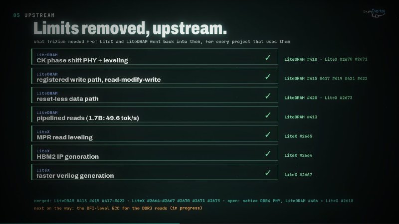
This is what we wanted from the project: a real, demanding workload on large boards, where every limit we hit in LiteX or LiteDRAM got fixed upstream rather than worked around locally.
Packing it into a ~$100 card: the YPCB-00338#
With the design correct, optimised and memory-bound on the large cards, it was time to see how small it could go. The Inspur YPCB-00338 is a retired data-centre card with a Kintex-7 XC7K480T, two 72-bit DDR3 channels (nine x8 chips each, 4 GB in total) and PCIe Gen2 x8. It sells second-hand for roughly $55 to $140. litex-boards already had a platform for it, after TiferKing’s documentation of the board, but LiteDRAM could not yet drive its DDR3 at full width.
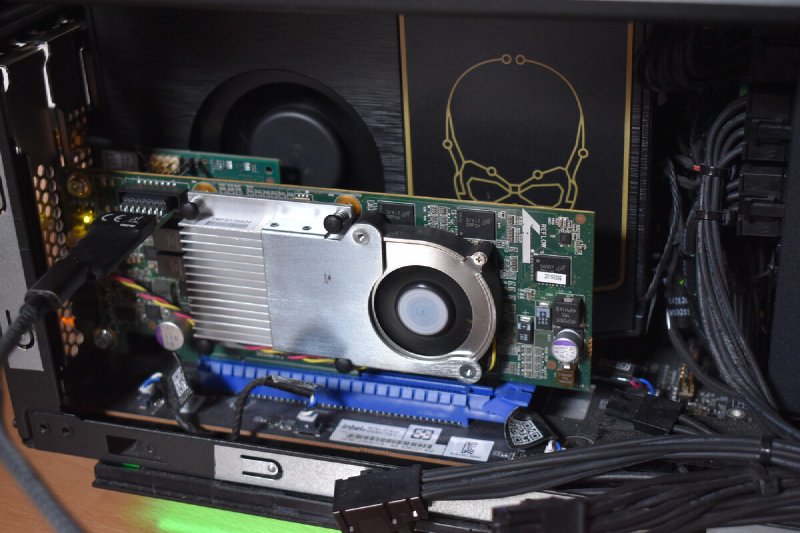
The difficulty is the DDR3 banks. They are high-range banks, which on 7-series have no output delay (ODELAY), so LiteDRAM’s 7-series PHY cannot do write leveling there. Each channel’s nine chips sit on a fly-by command and clock bus, so the clock reaches each chip at a different time, and with one static DQS phase only some of the lanes meet the DDR3 write timing. openTPU (FeSens) had documented a bring-up technique for this card: shift the phase of the clock itself instead, scan it finely, and check with real traffic at each step. We reimplemented it in LiteX and LiteDRAM:
- The PHY:
K7DDRPHYwith a CK phase shift mode (LiteDRAM #418): CK and the command pins on MMCM outputs with fine phase shift, the data on static outputs of the same MMCM, a per-lane write latency and a per-bit read framing. - The calibration: CK phase leveling in liblitedram (LiteX #2670, #2671), run by the SoC’s own CPU. The CK phase is scanned over one clock period in 16.7 ps steps; at each step a full calibration and a LiteDRAM BIST under traffic, and the channel settles in the middle of the longest passing run. The BIOS levels both controllers at boot.
- The board: both DDR3 channels at full width in the litex-boards target (#923, #924, #925).
Two bugs only the card could show came up on the way. The board has no DDR3 data mask pins, so the
engine’s 256-bit writes into 512-bit controller words stored the unwritten half as zeros: the
engine ports now read-modify-write their partial words, and the simulation models drop the masks
as the board does. And LiteX’s wishbone.Cache reversed the 32-bit words of each L2 line with its
default setting, which nothing had exercised on the other boards.
Packing came next. The YPCB-00338 got eight engine channels (four per controller) and a denser weight code: 5 trits per byte (3^5 = 243 fits in 256), 1.6 bits per weight instead of 2, so 20% fewer bytes to stream. Then a weight prefetch in the engine and fused vector instructions. All of it in 216k LUTs (72%) and 90% of the block RAM, timing met:
| build | change | 1.7B tok/s | 8B tok/s |
|---|---|---|---|
| simulation projection | four channels, 2-bit codes | 25.8 | 6.65 |
ypcb_up (14 Oct) | first PCIe run, four channels, 2-bit codes | 27.0 | 6.44 |
ypcb_t5n8c (15 Oct) | eight channels, 5-trit codes | 32.1 | 7.83 |
ypcb_pff2 (15 Oct) | weight prefetch, fused vector instructions | 35.2 | 8.11 |
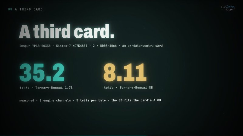
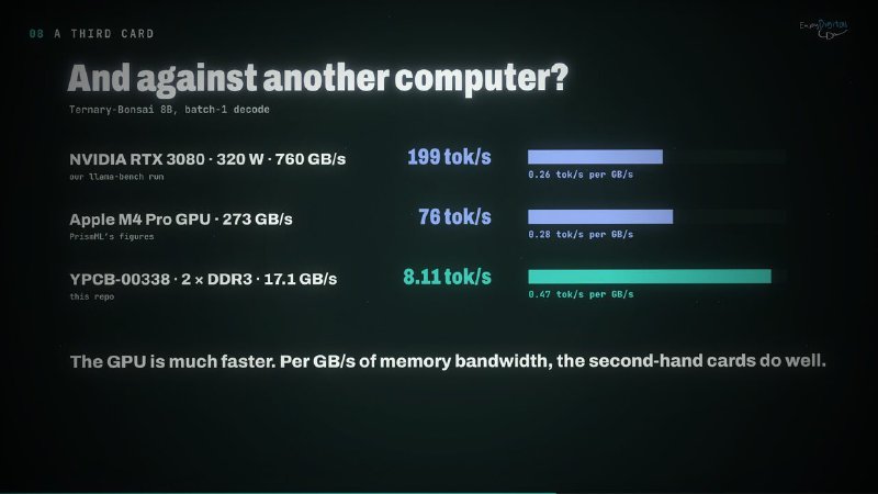
An 8B language model decoding at 8 tok/s, entirely on a card that costs less than the motherboard it plugs into, is the result we like best in this first part. Per GB/s of memory bandwidth, where batch-1 decode lives, the YPCB-00338 gets 0.47 tok/s out of each GB/s on the 8B, against 0.26 for an RTX 3080 and 0.28 for the M4 Pro’s GPU. The GPU is of course much faster in absolute terms; it also has 44x the bandwidth and a 320 W rating.
openTPU on the same card#
The YPCB-00338 has another open LLM accelerator: openTPU by FeSens, an int8/4-bit systolic design with an ISA and a compiler, which also uses LiteDRAM for its DDR3. That makes it a very good comparison: same card, same memory controller, both open, both essentially one person’s work (give or take an AI agent), and opposite trade-offs.
openTPU runs any off-the-shelf model through its compiler and keeps the DRAM busier (91 to 94% of the peak while decoding). TriXium only runs natively ternary models with a fixed engine, but reads about 3.5x fewer bytes per token, which comes out at 2.5 to 2.8x the decode rate per parameter on the 1.7B and 8B. Those are different models, so it is a speed comparison, not a quality one. The like-for-like comparison came later with the Bonsai 2 models, which are ternary versions of the same Qwen3.5 models openTPU runs at 4 bits: part 3 has the numbers. openTPU keeping its DRAM busier than we do is also a clear signal of where our remaining work is: the per-token serial work that does not overlap with the weight streams yet.
We also owe openTPU the DDR3 bring-up technique of this card, and it is nice to see LiteDRAM being used by another project on the same hardware, and tested there against AMD’s MIG.
What is not perfect yet#
On the cards, long generations are not always identical from one run to the next on two boards, and we would rather say so than let a demo hide it:
- YPCB-00338: when every channel streams at full rate, the DDR3 read eye of one controller is only 2 to 3 delay taps wide, and errors drift with temperature. A DFI-level SECDED ECC on the spare ninth byte lane is now in LiteDRAM (#423, litex-boards #928), and a DDR3-933 build cuts the errors about 400x.
- XCU1525: on some boots, one DDR4 controller trains on a marginal spot and corrupts writes. The fix is a boot-time deep memory test that retrains until it passes.
Both are memory margin problems the simulation cannot see, which is why the next work is as much about making correctness boring as about speed.
Try it#
TriXium is BSD-2-Clause, on GitHub. With a card and its
host described in ~/.config/trixium/boards.ini:
trixium deploy --board ypcb --model 1p7b   # bitstream, firmware, weights, tokens, bench
trixium chat                               # on the card's host: talk to it
trixium smi -l 1                           # and watch the engine and the memory channels
And without a card, the whole SoC (CPU, firmware, core, memory controllers) runs in Verilator:
trixium models --tiny && ./trixium_sim.py --build && ./trixium_sim.py --runThe bitstreams of this part are built with Vivado, the one closed piece with the FK33’s hard HBM2 controller. openXC7, the open flow for 7-series, is the natural next step for the YPCB-00338’s Kintex-7.
TriXium runs PrismML’s Bonsai models (on Qwen’s Qwen3 and Qwen3.5 architectures) from their GGUF files, with PrismML’s llama.cpp fork as the reference, and owes the idea of ternary LLMs to BitNet. Built on LiteX, LiteDRAM, LitePCIe, LiteX-Boards and VexiiRiscv. Thanks to FeSens for openTPU and its DDR3 bring-up technique, to TiferKing for the YPCB-00338 documentation, and to the crypto-mining community for giving these cards a second life.
Work and ideas by Enjoy-Digital; written up with AI in the loop.