

TL;DR: the DIPSY-40NX (Trenz article TEL0025) pairs a Lattice Certus-NX with 32 MB of HyperRAM. We brought it up in LiteX, tuned the HyperRAM core, fixed a burst bug that corrupted OpenSBI when it executed in place from HyperRAM, and booted Linux 6.9 on the result. The final target runs the SoC at 75 MHz; the bandwidth table keeps the original 50 MHz bring-up measurements so each HyperRAM change is compared at the same clock. 32 MB is enough.
The board#
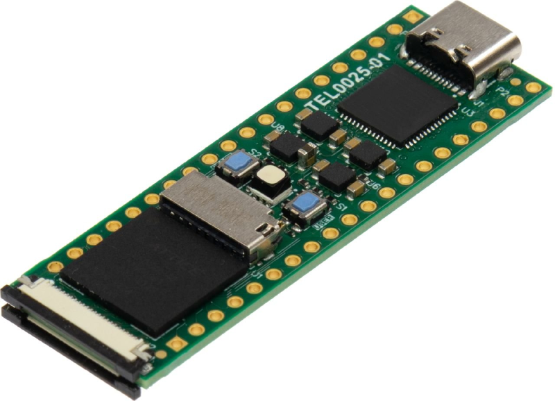
The board is the DIPSY-40NX, a DIP-form-factor module that reached our bench thanks to Trenz Electronic and Antti Lukats. TEL0025 is its Trenz article number; it is printed on the silkscreen and it is the name the LiteX target uses (the board is not listed in the Trenz shop yet as I write this). At its center sits a Lattice Certus-NX LFD2NX-40, a 40k-class part from Lattice’s Nexus family, built with the Radiant toolchain. Around it: a 25 MHz oscillator, an FT2232H for JTAG and serial, SPI flash, an SD card slot, two MIPI camera inputs, an RGB LED, and the star of this note, 32 MB of HyperRAM.
LiteX support landed in
LiteX-Boards in June as the trenz_tel0025 platform
and target. The board has a 25 MHz oscillator. In the committed target, an NXPLL turns that into
the 75 MHz system clock used by the CPU and LiteX SoC, plus a sys2x clock for the HyperRAM
core’s 2:1 mode. In that mode the HyperRAM CK itself is sys/2, so 37.5 MHz on the final
75 MHz target; sys2x is only the internal phase clock used by the PHY.
You will still see 50 MHz in the HyperRAM performance section below. Those are fixed-clock measurements from the earlier bring-up bitstream, kept because they show the effect of the core changes without mixing in a clock change. The Linux design described later is the 75 MHz one.
Main memory over thirteen pins#
A proper DDR controller wants a wide bus, length-matched traces and a serious PHY. On a small board with a small FPGA, HyperRAM is the pragmatic alternative: eight data pins, a strobe, a clock pair, chip select and reset, thirteen pins in total here, with a protocol simple enough that the whole controller is one readable Python file. The trade-off is bandwidth, which is exactly what the rest of this note is about.
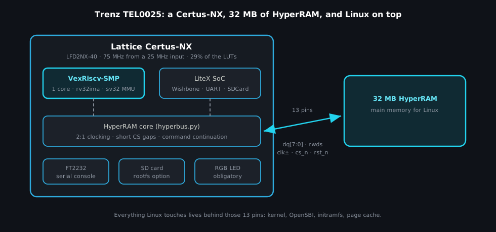
LiteX’s HyperRAM core lives in
litex/soc/cores/hyperbus.py
with Wishbone, AXI-Lite and AXI frontends. On the TEL0025 the target maps it as main memory with
one call:
# litex_boards/targets/trenz_tel0025.py
self.add_hyperram(
    region_name  = "main_ram",
    latency        = 7,
    latency_mode   = "variable",
    clk_ratio      = "2:1",
    cs_high_cycles = 2,
    size           = _HYPERRAM_SIZE,   # 32 MB.
)
The latency=7 here is deliberately just a conservative reset value. The core runs in
variable-latency mode and reports its configuration to software, and the BIOS reprograms the chip
at runtime based on the actual clock (3-clock latency at 85 MHz and below). That split keeps the
gateware generic and lets the software pick the timing.
Making it fast#
The first memspeed numbers came from the 50 MHz bring-up bitstream: 5.2 MiB/s write,
14.6 MiB/s read. The FPGA was not the bottleneck; the protocol overhead was. Every 32-bit access
paid a full command sequence, the access latency, and a long chip-select-high pause before the next
command could start. The optimization pass attacked all three, in three steps.
2:1 clocking#
The core’s default 4:1 clocking is safe and slow: the HyperRAM CK runs at a quarter of the
system clock. The 2:1 mode raises it to half the system clock, using the sys2x clock domain for
the PHY phases, which is why the CRG grew a second PLL output. This is the clk_ratio="2:1" in
the snippet above.
Shorter CS gaps#
Between two commands, the core held chip select high for 9 cycles. The datasheet asks for far
less, so we made the gap configurable (cs_high_cycles) and validated 2 cycles on the TEL0025
hardware. Together with the 2:1 clocking, this took memspeed to 11.1/22.7 MiB/s write/read.
Command continuation#
The big one. HyperRAM supports linear bursts: once a command is open, contiguous words can keep
streaming without paying a new command and latency each time. The core now keeps a read command
open when the next request is verified to target the next word, and does the same for adjacent
writes. Sequential traffic, which is most of what a CPU loading a kernel or running memcpy
generates, rides a single long command instead of thousands of short ones. Writes jumped to
46.7 MiB/s.
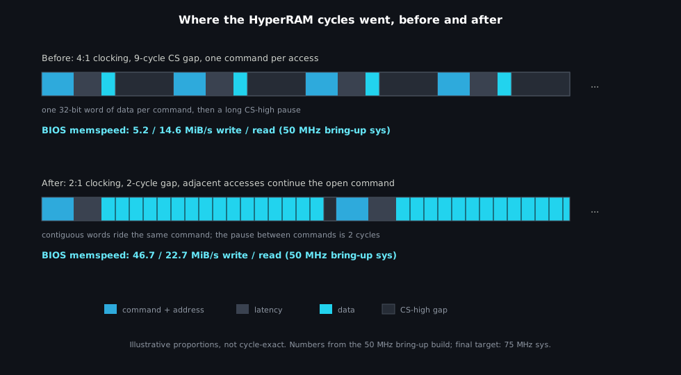
The measured progression below is a fixed-clock comparison: every row is a BIOS memspeed run on
that 50 MHz bring-up build.
| Configuration | Write (MiB/s) | Read (MiB/s) |
|---|---|---|
| Bring-up configuration (4:1 clocking) | 5.2 | 14.6 |
| 2:1 clocking, 2-cycle CS gap | 11.1 | 22.7 |
| + adjacent-access continuation | 46.7 | 22.7 |
Reads gain less than writes from continuation because every new read command still pays the initial access latency before data flows, and read traffic breaks contiguity more often. Still, a 9x improvement on writes and a decent bump on reads, without changing the board or raising that 50 MHz test clock: just fewer wasted cycles per useful word.
Making it correct#
The speedup was the easy half. The part that took actual care was keeping the optimization correct, because one workload is unforgiving here: OpenSBI executes in place from HyperRAM. There is no copy to a faster memory; the CPU fetches instructions straight through the core, and any wrong word is a crash or, worse, silent corruption.
An earlier iteration of the core auto-detected bursts: if two classic Wishbone accesses happened to be adjacent, they were merged into one HyperRAM burst. That heuristic corrupted execute-from-HyperRAM workloads. The fix that stuck is stricter, from the commit message:
Only keep a HyperRAM data command open when the current beat was explicitly accepted as an incrementing burst and the next request is contiguous. Adjacent classic Wishbone accesses must not be auto-detected as bursts, since that corrupts execute-from-HyperRAM workloads such as OpenSBI on the Trenz TEL0025 VexRiscv-SMP design.
So the frontend only continues a command for explicit incrementing bursts (Wishbone CTI) or for
a next request that is already valid and verified contiguous; it never guesses. A related fix
broke a combinatorial loop that Radiant flagged, where the HyperRAM response path fed back into
the Wishbone request path within one cycle.
Every step of this went in with regression tests in test/test_hyperbus.py,
and the end state was validated on hardware with clean OpenSBI boots and a full 32 MB BIOS
mem_test on the 75 MHz target. It is the same small-checkable-steps discipline from the
AI-era post: the simulation tests catch the logic mistakes in seconds, the
board confirms the timing, and an XIP firmware is the ultimate integration test. 🙂
Linux in 32 MB#
With the memory fast and trustworthy, the Linux part is almost routine, which is the point of
linux-on-litex-vexriscv. The TEL0025
entry there builds a single-core VexRiscv-SMP (rv32ima with an sv32 MMU) at 75 MHz, runs
Linux 6.9 built with Buildroot, and boots through OpenSBI 1.3.1 (the litex-hub
fw_jump build). The whole SoC uses 29% of the Certus-NX’s LUTs and 18% of its registers, so
there is comfortable room left for the actual application gateware next to it.
The interesting constraint is the memory budget. Here is how 32 MB is laid out at boot:
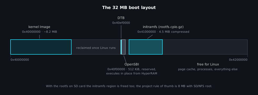
The SMP Linux variants place OpenSBI at main_ram + 0xf00000 with a 512 KiB reserved region, and
the target actually enforces the arithmetic: it refuses to build the Linux variant with less than
16 MiB of main RAM. The 32 MB HyperRAM clears that bar with half left over for Linux itself.
Making it fit#
32 MB stopped being a comfortable amount of RAM for Linux somewhere around a decade ago, so the default images needed a diet. Three changes did it:
Compress the initramfs. The Buildroot rootfs is 9.8 MiB as a plain cpio; gzipped it is
4.5 MiB, and the boot flow now loads rootfs.cpio.gz directly, with the post-image script
rewriting linux,initrd-end in the device tree to match. That is 5 MiB of HyperRAM back for the
price of a little decompression time at boot.
Trim the kernel. The LiteX console is a LiteUART; there is no display and no need for the
whole virtual-terminal layer. The kernel config now sets CONFIG_EXPERT and drops the unused
console machinery:
# CONFIG_VT is not set
# CONFIG_UNIX98_PTYS is not set
# CONFIG_LEGACY_PTYS is not set
# CONFIG_FRAMEBUFFER_CONSOLE is not set
# CONFIG_LOGO is not set
Move the rootfs off RAM entirely. The board has an SD slot and the SoC has LiteSDCard, so
--rootfs=mmcblk0p2 boots with root=/dev/mmcblk0p2 and no initramfs resident in RAM at all.
The project README’s rule of thumb applies: 32 MB for a self-contained RAM boot, and as little as
8 MB when the rootfs lives on SD or NFS.
Try it#
The flow is the standard linux-on-litex-vexriscv one, with the TEL0025 as the board:
git clone https://github.com/litex-hub/linux-on-litex-vexriscv
cd linux-on-litex-vexriscv
./make.py --board=trenz_tel0025 --build --load
litex_term /dev/ttyUSB1 --images=images/boot.json
Add --rootfs=mmcblk0p2 to make.py for the SD-card root variant. The board itself is the
limiting factor for now: until Trenz lists it, this note is mostly useful as a recipe for any
Certus-NX (or other small FPGA) with a HyperRAM hanging off it, and the HyperRAM core
improvements apply to every LiteX board that uses one.
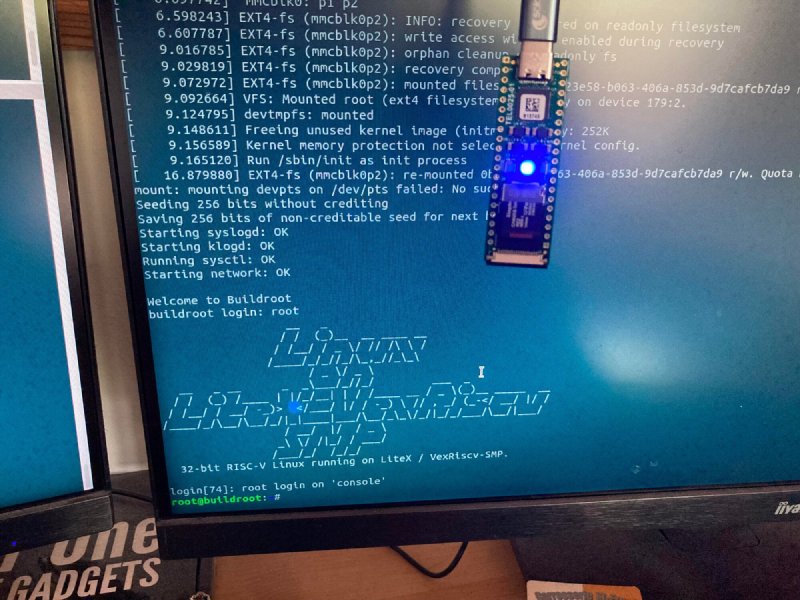
We posted the quick test on X when it first booted, board dangling in front of its own console included. The performance numbers in this note are the ones recorded in the commit messages at validation time; a proper text boot log with timing measurements is on the list for a follow-up note.
Built on LiteX, LiteX-Boards and linux-on-litex-vexriscv. The DIPSY-40NX / TEL0025 board came to us thanks to Trenz Electronic and Antti Lukats; the LiteX HyperBus core also carries contributions from MoTeC.
Work and ideas by Enjoy-Digital; written up with AI in the loop.