
TL;DR: LiteDRAM has a new PHY, NXRPCPHY, for
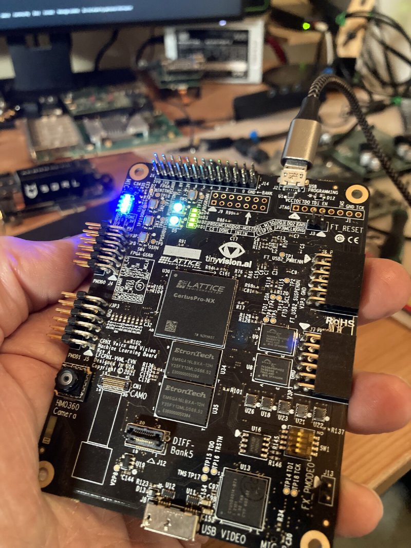
Etron’s RPC DRAM on Lattice CertusPro-NX. It is validated on the CertusPro-NX Voice and Vision
Machine Learning (VVML) board designed by tinyVision.ai: the BIOS memory
test passes from sys_clk 50MHz to 100MHz (800MT/s at the pins), and the BIST of LiteDRAM writes and
reads at about 1280 MiB/s with Address Streaming, 84% of what the bus can carry. Both DRAMs of the
board are used, for 64 MiB. The base of the PHY is the RPC DRAM work Antmicro did on Xilinx
7-Series in 2021. We ported it to the Nexus IO primitives and extended the controller for what
this memory expects.
What RPC DRAM is#
RPC DRAM (Reduced Pin Count DRAM) is a memory from Etron that gives DDR3-class bandwidth on 22 or 24 pins. A 16-bit DDR3 chip needs more than 40 signals: data, strobes and masks, plus a separate bus for the address, the bank and the command. RPC DRAM removes that second bus completely:
| Pin | Role |
|---|---|
CLK, CLK# | Differential clock |
CS# | Chip select |
DQS, DQS# | Differential data strobe (one pair, or one per byte) |
DB[15:0] | Data, and the parallel commands |
STB | Serial commands |
The commands travel on the data pins. A transaction starts with a Request Packet, sent in parallel
on DB. The commands that follow it are Serial Packets, sent bit by bit on the single STB line
while DB is busy with data. Data moves in WORDs: a burst of 16 beats of 16 bits, 32 bytes, over 8
clock cycles (tCK), on both clock edges as in DDR3.
The chip on the VVML board, the EM6GA16L, is a 256Mb part (32 MiB, 4 banks) in a small BGA. For an FPGA like the CertusPro-NX, that means a few tens of megabytes of fast RAM for about half the IOs of a DDR3 interface, routed on a small board. The cost is in the PHY and the controller: RPC DRAM looks like DDR3 from far away, but its command protocol, its refresh and its initialization are its own.
The starting point: Antmicro’s PHY#
LiteDRAM has had an RPC DRAM PHY since 2021, written by Antmicro (LiteDRAM #273). It introduced a structure that the LPDDR4 and LPDDR5 PHYs later reused: a base PHY that holds the protocol (the translation of the DFI commands of the controller into Request and Serial Packets, the preambles, the initialization state machine) and a backend per FPGA family that only serializes the result to the pins.
No board with RPC DRAM existed at the time. Antmicro tested the Artix-7 backend on an Arty A7
whose DDR3 chip had been replaced by a pin-compatible RPC DRAM, with the power management IC
reprogrammed over I2C to supply 1.5V instead of 1.35V. It worked, but hardware issues on that
modified board (possibly the termination of CS# and STB) kept it at low frequency, and the PHY
stayed in that state.
The VVML board changes the situation: two EM6GA16LBXA-12H wired to a 1.5V bank of a CertusPro-NX (LFCPNX-100), with proper routing. The board has been in LiteX-Boards since 2024, and until this week the SoC ran from block RAM only.
The Nexus backend#
The base PHY keeps its 1:4 ratio between the controller clock and the DRAM clock: at sys_clk
100MHz, CLK runs at 400MHz and the pins toggle at 800MT/s. The new backend, NXRPCPHY, maps that
to the Nexus IO primitives. The 7-Series backend could not serve as a model here, because the two
families do not offer the same things.
One edge clock. The 7-Series backend uses two phase-shifted copies of the fast clock. On
Nexus, the fast IO logic runs on an edge clock, a dedicated low-skew clock along an IO bank, and
the gearboxes (the X4 serializers and deserializers, 8 bits per sys_clk cycle) derive the system
clock from it with an ECLKDIV. The backend uses a single edge clock, sys4x. CLK and DQS are
aligned to it. DB has to be centered on CLK, so it is sent 90 degrees ahead with the write
clocks of the DQSBUF, the Nexus primitive that manages a strobe group. STB and CS# are plain
outputs and get their quarter cycle from an output delay line.
Reads with the DQS of the DRAM. The 7-Series backend samples the read data on the FPGA clock.
On Nexus, a pin can only be bidirectional at X4 gearing with the memory primitives: Radiant does
not pack a generic input deserializer with an output one on the same pin. So reads are captured
with the strobe the DRAM sends back, through the DQSBUF, as the DDR3 PHY of LiteDRAM for Nexus
already does. The DQSBUF needs a READ signal that opens a gate on DQS during its preamble and
keeps it open for the 8 tCK of the burst. It then returns the burst aligned on sys_clk, over two
cycles flagged by DATAVALID.
Alignment by CSRs. The output primitives do not have the same latency: for the same input,
DB comes out 3 UIs after DQS (a UI, unit interval, is one bit time: half a tCK) and STB/CS#
5 to 6 UIs after it. Each group has a write shift, in UIs, and the position of the READ gate is
adjustable too. All of them are CSRs, so they can be scanned from software during the bring-up and
then frozen as defaults.
On the target side, it is used like any other LiteDRAM PHY:
self.ddrphy = NXRPCPHY(
    pads         = platform.request("rpcdram"),
    sys_clk_freq = sys_clk_freq)
self.add_sdram("sdram",
    phy    = self.ddrphy,
    module = EM6GA16L(sys_clk_freq, "1:4"))
Bring-up: simulation first, then the board#
With five signal groups to align and a DRAM that stays silent when a command is wrong, we did not
start on the board. The repository now has a simulation of the bare PHY with Lattice’s own
primitive models (the QuestaSim shipped with Radiant) against a timing-aware RPC DRAM model
(bench/rpc/sim). It replays the initialization of the BIOS, reads the Utility Register of the
DRAM (a register that returns known patterns, made for this) and does a write and a read. The first
write shifts and READ position came from there.
On the board, a small script, rpc_console.py, does the same through the BIOS console: it takes
the DRAM under software control, moves one parameter, writes a WORD, reads it back and prints a
map. No extra bridge or probe is needed, only the serial port. The simulation was close but not
exact: STB/CS# need one more UI on the board.
A second behavioural model, in Migen, sits behind the simulation PHY of LiteDRAM. With it, the simulation SoC runs the BIOS initialization and memory test in Verilator, so the controller changes below could be tested without hardware.
What the DRAM asked for#
The PHY was the smaller part of the work. Most of the fixes were about how this memory wants to be driven, and several of them are in the controller, not in the PHY.
Refresh is a burst, not a tick. The module description used DDR3-like values: a refresh every 7.8µs. An RPC DRAM refresh command refreshes all the rows of the selected banks, 100ns per row, and the DRAM accepts nothing until it is done. With the DDR3 values the DRAM was permanently busy and ignored the commands. The module now refreshes the 4 banks in one burst every 32ms. The burst lasts 1.64ms nominally; the time the controller waits for it was increased later, for a reason that only appeared with two DRAMs (see below).
One Request Packet at a time. LiteDRAM’s multiplexer can place an activate or a precharge on
one phase while a read or a write goes on another. RPC DRAM takes a single command stream: each
Request Packet is followed by 8 tCK on STB, and a read or write has to finish, latency and burst
included, before the next packet. For the RPC memory type, the multiplexer now sends all the
commands through one path, with these spacings.
The read position depends on the frequency. The round trip from the command to the returned
DQS, counted in tCK, is not the same at 200MHz and at 400MHz, so a fixed READ position only
fits one frequency. The read leveling of the BIOS now scans it: for each of 8 positions of 1 tCK,
it scans the read clock selection of the DQSBUF and keeps the position with the widest window.
The DQS path is already long at 400MHz. The DQSBUF delays DQS by 90 degrees to sample in
the middle of the bit. At CLK 400MHz, its own path is already about one UI long, so with the
90 degrees on top each edge captured the data of the next UI and the first word of the burst was
lost. After the initialization, the PHY now decreases that delay.
Reset the gearboxes with the clock stopped. At this point 50MHz and 100MHz worked, and 75MHz
did not: the DRAM did not answer at all. The gearboxes and the DQSBUFs were reset with the system
reset, released a few cycles after the edge clock restarts. They did not all start on the same
edge clock cycle, so the alignment between STB, DQS and DB depended on the frequency. They
are now reset by the initialization sequence, while the edge clock is stopped, like the ECLKDIV.
STB and CS# arrive late. A map of the working STB/CS# delays at each frequency showed a
constant offset: the two signals arrive about 450ps later than expected. With the textbook quarter
cycle they were at the edge of their window at 400MHz. The delay is now tCK/4 less this skew,
which puts it in the middle of the measured window at every frequency:
| CLK | Working delays (taps of about 12.5ps) | tCK/4 | Delay used |
|---|---|---|---|
| 200MHz | 0 to 127 (the whole delay line) | 100 | 64 |
| 300MHz | -13 to 88 | 67 | 31 |
| 400MHz | -20 to 48 | 50 | 14 |
| 450MHz | -25 to 40 | 44 | 8 |
CS# before a reset. After a second initialization from the BIOS prompt (sdram_init), about
half of the 2 MiB memory tests had one or two wrong words. CS# had stayed low since the first
initialization. The DRAM wants to see it go high then low before a reset, and the PHY now does
that.
Results#
The first results are with one DRAM of the board. The BIOS memory test passes from sys_clk 50MHz to 100MHz, with the same settings, and Radiant meets timing:
| sys_clk | CLK | Rate | Memspeed write | Memspeed read |
|---|---|---|---|---|
| 50MHz | 200MHz | 400MT/s | 17.5 MiB/s | 26.4 MiB/s |
| 75MHz | 300MHz | 600MT/s | 26.6 MiB/s | 38.8 MiB/s |
| 100MHz | 400MHz | 800MT/s | 33.9 MiB/s | 50.7 MiB/s |
SDRAM:		32.0MiB 16-bit @ 800MT/s (CL-9 CWL-9)
Read leveling:
  m0, b03: |0000000001111111| delays: 12+-03
  m0, b04: |0111111110000000| delays: 04+-03
  best: m0, b04 delays: 04+-03
  m1, b03: |0000000000111111| delays: 12+-02
  m1, b04: |0011111111000000| delays: 05+-03
  best: m1, b04 delays: 05+-03
Memtest at 0x40000000 (2.0MiB)...
Memtest OK
Memspeed at 0x40000000 (Sequential, 2.0MiB)...
  Write speed: 33.9MiB/s
   Read speed: 50.7MiB/s
In the read leveling lines, b03 and b04 are two READ positions and each character is one read
clock selection: position 4 gives a window of 8 steps out of 16 on both bytes. A mem_test
over the whole 32 MiB also passes.
The memspeed numbers measure the CPU of the SoC more than the memory. The BIST of LiteDRAM, a generator and a checker in the fabric, gave 358 MiB/s in write and 355 MiB/s in read at 100MHz, with sequential and random addresses and no error over 26.4 GiB each. That is the limit of a controller that sends one Request Packet per WORD: 32 bytes every 8 to 9 sys_clk cycles, when the bus can carry 1526 MiB/s.
Address Streaming#
RPC DRAM has a mode for exactly this, and it is the reason STB exists. After the Request Packet
of a read or a write, a Serial Packet on STB every 8 tCK gives the next address, in any bank with
an open row, at any column. The WORDs then follow each other on DB without a gap, and a Burst
Stop ends the stream.
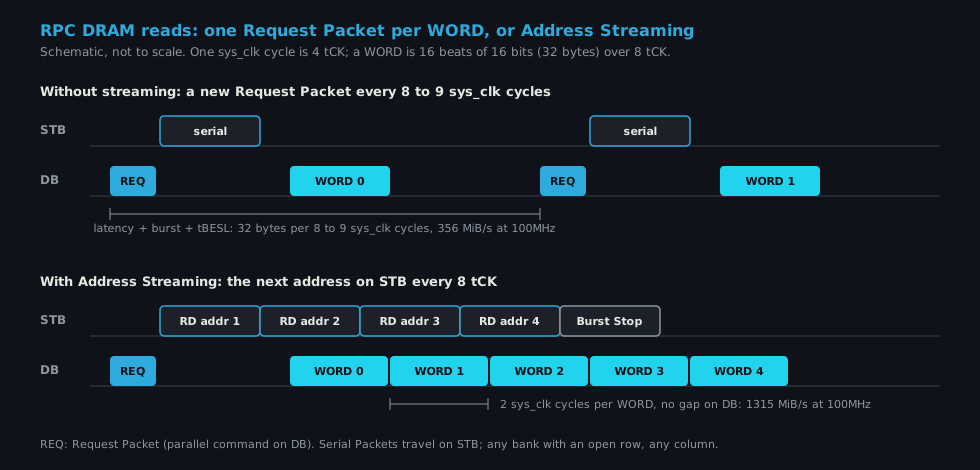
Two changes implement it. The multiplexer accepts the next read or write of the same type exactly 2 sys_clk cycles after the previous one, instead of waiting for the end of the burst. The PHY sees that spacing, sends the command as a Serial Packet and adds the Burst Stop when nothing follows. Activates, precharges and refreshes still end the stream.
Same bitstream at sys_clk 100MHz, streaming switched with a CSR of the controller:
| Read streaming | Write streaming | Write | Read |
|---|---|---|---|
| off | off | 356 MiB/s | 356 MiB/s |
| on | off | 356 MiB/s | 1310 MiB/s |
| off | on | 1318 MiB/s | 355 MiB/s |
| on | on | 1315 MiB/s | 1313 MiB/s |
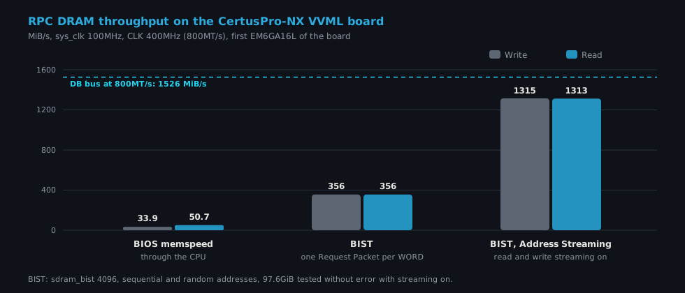
That is 3.7 times faster, with 97.6 GiB tested without error with both directions on. The BIOS
memory test and mem_test also pass in that configuration.
There is one restriction on writes. In a stream, the DRAM only takes the write masks of the first
and of the last WORD. Write streaming is therefore only valid when full WORDs are written, which
is the case for the BIST and for a CPU that goes through the L2 cache of LiteX, but not for an
arbitrary user port with byte enables. Read streaming is on by default, write streaming is off,
and both are settings of the controller (read_streaming, write_streaming) that the streaming
CSR can change at run time.
Two DRAMs on one bus#
The board has two EM6GA16L. They share CLK, DQS and DB, and each one has its own STB and
CS#: what DDR3 calls ranks, and what the RPC DRAM datasheet calls Multi Rank. The PHY now takes a
nranks parameter, and with --rpc-ranks 2 on the target the BIOS reports 64 MiB.
CS# selects the DRAM that takes a command, and it also enables its termination, so it is only
low on the DRAM of the current command. When the controller moves to the other DRAM, the PHY
lowers its CS# with the STB preamble and raises the CS# of the previous one a sys_clk cycle
later. A stream stays in one DRAM: the multiplexer ends it when the rank changes. Refresh,
precharge and the initialization commands go to both DRAMs at once. The read leveling is done on
the first DRAM. The window of the second one is one delay step later, well inside the margin.
Sharing the bus exposed two things that a single DRAM had hidden.
A refresh ends when the DRAM says so. The refresh burst is timed by the DRAM itself, 100ns per
row, with no tolerance in the datasheet, and the DRAM drives DQS high until it is done. With the
controller waiting the nominal 1.64ms plus 2µs, about 1 read in 10000 of the first DRAM had a
wrong bit in its first data: the second DRAM was still driving DQS at the end of its refresh.
The controller now waits 1.5 times the nominal duration, 2.46ms every 32ms.
An unused DRAM still has to be reset. With two DRAMs on the board and only one used, the other
one was left alone. Once configured by an earlier bitstream, it keeps its state when the FPGA is
loaded again, and the read leveling of the first DRAM then failed completely. The PHY now sends
the reset sequence to every DRAM on the bus and keeps the CS# of the unused ones high afterwards.
The longer refresh costs a little throughput: with the same test as above, the BIST gives
1281 MiB/s in write and 1278 MiB/s in read, 84% of the bus, with one DRAM or two. With both DRAMs
at sys_clk 100MHz, the BIOS memory test and mem_test over the 64 MiB pass after each of 6
bitstream loads, and the BIST ran 73 GiB at random addresses without error.
Limits and next steps#
- 900MT/s does not pass. sys_clk 112.5MHz (
CLK450MHz) meets timing, but reads have rare bit errors on the lower byte and no read window on the upper byte. 125MHz does not meet timing in the SoC. - 4 DFI phases. A burst spans two controller cycles. With 8 phases it would fit in one, which would simplify the base PHY. It is the main item of the rewrite list in the README of the PHY.
- More serial commands. Serial activate and precharge, and Toggle RW, would keep a stream alive across a row change or a change of direction.
- Radiant only. The backend uses the Nexus memory primitives and has been built with Radiant.
Try it#
# LiteX SoC on the CertusPro-NX VVML board with the two RPC DRAMs as main RAM (64MiB) and the
# BIST (Radiant).
python3 -m litex_boards.targets.lattice_certuspro_nx_vvml --with-rpcdram --rpc-ranks 2 --with-bist \
    --csr-csv csr.csv --build --load
litex_term /dev/ttyUSBX

# From the BIOS: sdram_bist <burst_length> <random>, sequential (0) or random (1) addresses.
litex> sdram_bist 4096 0
litex> sdram_bist 4096 1

# Bring-up maps through the BIOS console (close litex_term first, run sdram_init afterwards).
./bench/rpc/rpc_console.py --csr-csv csr.csv --port /dev/ttyUSBX stbmap
./bench/rpc/rpc_console.py --csr-csv csr.csv --port /dev/ttyUSBX rdmap

# No board: BIOS memory test and BIST against the RPC DRAM model in Verilator.
python3 litedram/phy/rpc/simsoc.py
python3 litedram/phy/rpc/simsoc.py --bist-length 16384 --stream-writes
python3 litedram/phy/rpc/simsoc.py --nranks 2 --bist-length 32768 --stream-writes
The work is merged: LiteDRAM #507 (Nexus backend, DRAM model, controller changes), #508 to #512 (bench scripts, frequency, resets, delays), #514 (Address Streaming) and #516 (two DRAMs), and LiteX-Boards #966 to #968 and #971 for the target. The details are in the README of the PHY.
Thanks to Antmicro for the original RPC DRAM PHY: the base PHY, the command encoding and the initialization are theirs, and the port would have been a much longer project without them. Thanks to tinyVision.ai and Lattice for a board that has this memory on it.
Work and ideas by Enjoy-Digital; written up with AI in the loop.