

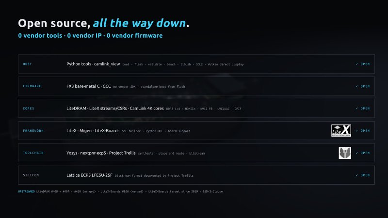
TL;DR: The Elgato Cam Link 4K is a popular HDMI to USB 3.0 capture card with a Lattice ECP5, a Cypress FX3 and 128 MB of DDR3 inside. In 2019 we added it to LiteX-Boards and booted Linux on it, mostly as a way to test its DDR3 with the open ECP5 flow, and that is where it stopped: replacing the product’s firmware was a team-sized project. This time it took a week. CamLink 4K is open gateware and firmware for the same device: one LiteX Python script built with Yosys, nextpnr and Project Trellis, a bare-metal FX3 firmware with no vendor SDK, 4K30 NV12 through an open DDR3 frame buffer, HDMI audio, and lines streamed as they arrive, so frames reach applications in 19 ms instead of 46 ms with the stock firmware. To get the frame buffer bandwidth we doubled the DDR3 rate of LiteDRAM’s ECP5 PHY, and that is now upstream for every ECP5 board.
2019: a LiteX board, and Linux as a RAM test#
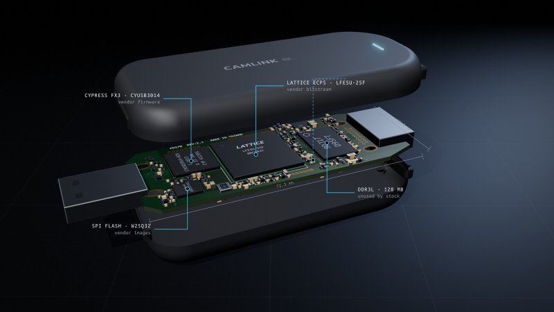
The Cam Link 4K got the attention of the open hardware community early. Inside its USB stick shell there is an ITE IT6802 HDMI receiver, a Lattice ECP5 LFE5U-25F, a Cypress FX3 USB 3.0 controller with an ARM9 core, 128 MB of DDR3L and an SPI flash. The ECP5 was the interesting part: it was the FPGA that Project Trellis had recently documented, in a cheap, mass-produced device. ktemkin wrote an FX3 exploration firmware and a host tool that could load a bitstream into the FPGA, and Greg Davill and the apertus° team traced the board netlist.
With that, the Cam Link 4K became a LiteX board. The LiteX-Boards target was written in 2019 and published in January 2020, and on the same day the board joined Linux-on-LiteX-VexRiscv: a VexRiscv at 81 MHz, the 128 MB of DDR3 as main memory through LiteDRAM’s ECP5 PHY, and a serial console on an LED pin wired out by hand, booting Linux. The first builds still went through Lattice Diamond; by March 2020 the workaround was gone and the board was built with Yosys, nextpnr and Trellis like the others.
Linux was a test more than a goal. Booting a kernel and a userspace exercises the DRAM, the PHY calibration and the whole open ECP5 flow harder than a memtest does, on hardware anyone could buy. Others worked on the stock firmware itself, like Mike Walters, whose 2020 patch made it play nicer with Linux video apps. But nobody replaced it. That would have meant a USB 3.0 firmware for the FX3 without its SDK, a driver for an HDMI receiver without a datasheet, the FPGA-to-FX3 streaming interface, a UVC implementation, audio, and a frame buffer in DDR3 at a rate LiteDRAM’s ECP5 PHY could not reach. For a small company, months of that work on a capture card that already worked were impossible to justify. The board stayed a LiteX target.
2026: the same board, the whole product#
At the end of September we came back to it with a different way of working, the one described in FPGA development with LiteX in the AI era: an AI agent does the implementation and runs the loops on the hardware, and we give the direction, the ideas and the review. The repository went from its first commit on a Monday afternoon to a released, documented capture card on Friday lunchtime, in 115 commits.
The plan had ten phases, each on top of the previous one: a bare-metal FX3 “hello”, FPGA configuration from the FX3, USB streaming, the GPIF-II interface between the FPGA and the FX3, UVC, the DDR3 frame buffer, HDMI capture, audio, and then the features the stock firmware does not have. Every step followed the same loop: implement, simulate (Migen and pytest, down to an end-to-end model from HDMI to UVC frames), test on the hardware with a script, document, commit.
The loop only works if the hardware can be driven and observed without a human in the middle, so
the host tools were written for that from the start. software/camlink.py boots the device,
loads bitstreams, reads and writes FPGA CSRs, flashes and recovers; the capture card’s own UVC and
UAC outputs give video and audio back; software/validate.py runs 12 hardware checks. The risk
was also low by construction: the FX3 boot ROM always falls back to its USB bootloader, so a broken
firmware is recoverable, and the stock firmware of the unit can be loaded into RAM in a few
seconds for side by side comparisons without touching the flash.
The plan, the decisions and the reviews were ours. The pieces where a team would have spent the months were where the agent did most of the work: an FX3 firmware written against register definitions (from Marcus Comstedt’s fx3lafw) instead of the Cypress SDK, an IT6802 init sequence rebuilt from the state the stock firmware leaves it in, and the long series of build, load and measure iterations on the DRAM.
What is in the design#
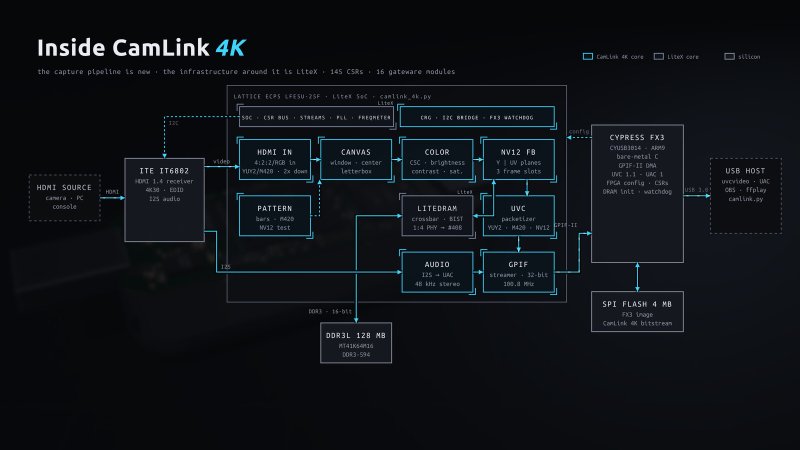
The ECP5 runs one LiteX SoC described in camlink_4k.py. Video from the IT6802 is captured
(HDMIIn, both its single and double data rate modes for 1080p60 and 4K30), cropped or scaled
(Canvas), colour adjusted, optionally written to DDR3 as NV12 planes, packetized as UVC payloads
and sent to the FX3 with the I2S audio over GPIF-II, a 32-bit synchronous parallel bus at
100.8 MHz. The FX3 firmware, about 4,700 lines of bare-metal C, configures the FPGA from the SPI
flash, initializes the DRAM through the FPGA’s CSRs, and presents UVC 1.1 video and UAC 48 kHz
audio to the host. Standard drivers do the rest: uvcvideo, ffmpeg, OBS, VLC.
What it delivers today: 4K30 as NV12 through the frame buffer or as M420 without it, 1080p60 YUY2, 720p and 480p, a 2x2 box downscale from 4K to 1080p instead of line dropping, a pixel-exact 1080p crop window anywhere in a 4K input, brightness, contrast and saturation, input information and crop control through a UVC extension unit, bit-exact HDMI audio, our own EDID, standalone boot from flash, and two watchdogs (the FPGA resets the FX3 if it hangs, the FX3 falls back to its bootloader if a firmware never enumerates). All of it built with open tools.
The DRAM, from a Linux test to a 4K frame buffer#
The stock firmware streams 4K30 as NV12, the format most applications want. NV12 stores the whole luma plane and then the whole chroma plane, while HDMI delivers both line by line, so it needs a frame buffer: each frame is written to DDR3 and read back, about 373 MB/s each way, 746 MB/s in total, with the USB side busy for most of each frame.
The DDR3 chip can do it: on a -8 ECP5, the DDR edge clock goes up to 400 MHz, DDR3-800, 1.6 GB/s peak. LiteDRAM’s ECP5 PHY could not. It used 1:2 gearing, meaning the DRAM clock runs at twice the controller clock, and with a controller and a SoC closing timing around 80 to 100 MHz on this FPGA, that is DDR3-324 to 400. Measured at DDR3-300, a writer and a reader running together got 395 MB/s, half of what NV12 needs. This was the configuration Linux ran on in 2020, and it was fine for a CPU.
The fix was a 1:4 mode: the controller keeps its clock, the PHY runs at twice that, and the DDR
edge clock at four times. LiteDRAM already had a generic DFIRateConverter for this on the 7-series
PHY; the ECP5 PHY needed a clock domain crossing for its CSRs, a CRG built on the ECP5’s edge clock
synchronizers and dividers, and the converter wired around it. That part worked on hardware the
next day, once the controller read latency was set one cycle lower than the generic estimate.
The rest of the time went into two problems that only showed up across builds:
- DRAM dead on about one build in eight. The converter’s crossing between the controller clock
and the PHY clock sampled each word on both edges of the faster clock, and with the ECP5’s clock
dividers the edges are either coincident or a quarter period apart: a hold race or 3.4 ns of
setup, on paths nextpnr does not check. A new
RateCrossingcaptures each word once per cycle on a CSR-selected edge and realigns the read data at runtime: 8 loads out of 8. - Still dead on about one build in five. The reset of the IO gearboxes came from the system reset, released with the edge clock running, and routed with more skew than an edge clock period on some placements: the pins came out of reset on different edges. Driving that reset from the PHY init sequence, released while the edge clock is stopped as Lattice’s sequence intends, fixed it: 9 loads out of 9 on three placement seeds. This one probably explains random DRAM failures on other ECP5 boards at 1:2 as well.
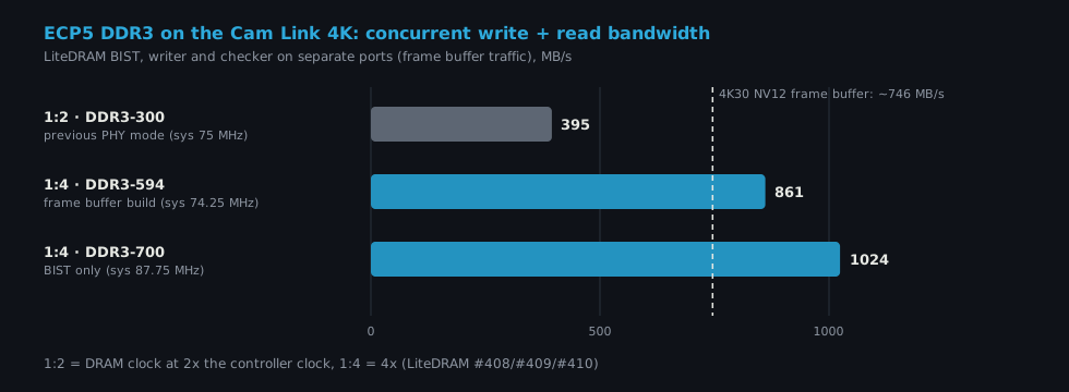
At DDR3-594 the BIOS memtest and a 64 MB BIST pass with 861 MB/s of concurrent traffic, and DDR3-700 reaches 1024 MB/s. DDR3-796 does not find a read window yet, while the stock Lattice IP runs DDR3-800 on the same board; the fine read delay of the ECP5’s DQS buffer, which LiteDRAM does not use, is the next thing to try. The frame buffer runs at DDR3-594 with margin, once its DRAM accesses were grouped into 64-word bursts: with single accesses, the crossbar switched banks between the writer and the reader on almost every access and 4K30 ran at 15 fps.
All of it is upstream and the CamLink 4K gateware uses the upstream PHY:
| PR | What |
|---|---|
| LiteDRAM #408 | ECP5 PHY CSR clock domain crossing, ecp5ddrphy_with_ratio() for 1:4, tests |
| LiteDRAM #409 | IO gearing reset from the init sequence (io_rst_init) |
| LiteDRAM #410 | RateCrossing for the 1:4 controller/PHY crossing |
| LiteX-Boards #866 | camlink_4k --sdram-rate 1:4 |
The same CRG pattern applies to the other ECP5 DDR3 boards in LiteX-Boards (ECPIX-5, OrangeCrab, ButterStick, Versa, TrellisBoard), so they can double their memory bandwidth with the open toolchain too, and the IO reset fix is worth having on all of them.
In 2020 the DDR3 held a Linux kernel. Now it holds three 4K frames for a pipeline running at the
same time, and the CPU is still there when we want it: --with-cpu adds a VexRiscv and the LiteX
BIOS next to the video path, with the same LiteDRAM behind both. Software that works on the frames
themselves, overlays, a freeze frame, an instant replay buffer, is now a matter of writing it.
Lines, not frames#
The stock firmware buffers whole frames: the first data of a frame leaves the device about two frames after the source drew it, then the frame goes out as a burst. CamLink 4K does not need a frame buffer for 1080p60 YUY2, so it sends each line about 1 ms after the HDMI receiver delivers it. The first data of a frame is on USB 3.5 ms after the source rendered it, and the frame reaches the application when its last line has been scanned.
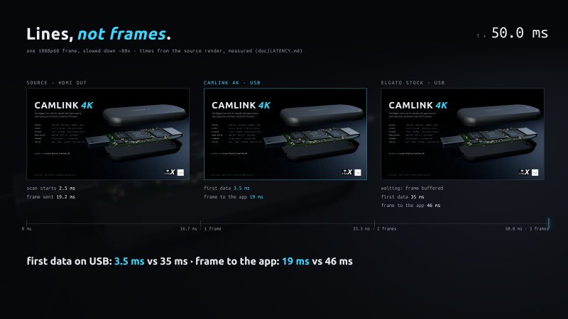
To measure it, the bench host draws a barcode with its own monotonic clock on its HDMI output and captures it back through the Cam Link, so a single clock timestamps every stage. With the same unit, cable and source, the frame is delivered to applications through uvcvideo in 19 ms instead of 46 ms with the stock firmware, and in 64 ms with a cheap MS2109 USB capture stick.
Past the device, most of the latency is in the display path. ffplay alone adds about 50 ms even
with its low latency options, so we wrote camlink_view, a small libusb and SDL viewer that draws
rows as they arrive. In a desktop window, the frame is on screen 35 to 38 ms after the source
rendered it, against 68 to 70 ms for the same viewer with the stock firmware. With direct display
through Vulkan, which bypasses the compositor, it is 19 to 30 ms, and the remaining spread is
the phase between the source and the display scanouts.
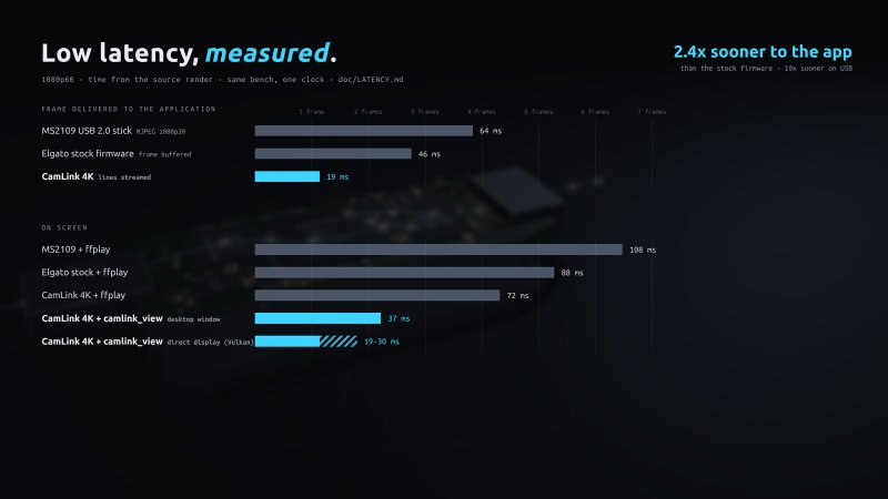
That remaining stage is also why the project has a design note on LitePCIe video cards: the capture side is close to the minimum, and only an output whose timing we control, phase locked to the input, removes the wait for the display scan. The same measurements frame where an open, low latency capture fits next to IP-KVMs, whose published figures range from 35 to 230 ms.
Best of both worlds#
This project is a good example of what changes and what does not. What changed is the cost of the implementation. The FX3 firmware, the IT6802 driver, the GPIF timing, the DRAM bring-up builds and the latency campaigns are the kind of work that needed a team over months in 2020, and it fit in a week with an agent doing the implementation, the hardware loops and the documentation.
What did not change is where the decisions come from. Going to 1:4 instead of trying to squeeze the 1:2 PHY, streaming lines instead of frames, keeping the frame buffer only for NV12, measuring latency against the stock firmware on the same unit instead of trusting published numbers, and pushing the PHY work upstream so every ECP5 board benefits: those are engineering choices from years of LiteX and FPGA work, and the agent made them cheap to try. The upstream PRs went through the usual review. The open flow mattered too: a Python design, open tools and scriptable hardware are what let an agent close the loop at all.
Limits#
- 1st gen only. The Cam Link 4K (
0fd9:0066); the MK.2 and Rev.3 are different designs. - 4K30 maximum. The IT6802 is an HDMI 1.4 receiver. 4K30 YUY2 does not fit in the USB 3.0 bandwidth, hence NV12 or M420. NV12 through the frame buffer can add up to a frame of latency.
- No HDCP sources.
- Test USB ID. It uses the pid.codes test PID
1209:0001for now. - DDR3-594, not 800. Enough for the frame buffer, with the faster rates as the next DRAM work.
- Firmware replacement. It replaces the FX3 image in the flash. Back up the whole flash first: it holds the stock firmware, which we cannot distribute, and the unit’s serial number. The README has the backup, install and back-to-stock steps.
Try it#
Following the README (Linux host, LiteX with an
up-to-date LiteDRAM, the open ECP5 toolchain, arm-none-eabi-gcc), after backing up the flash with
cl4k-fwtool and installing the
CamLink 4K FX3 image:
git clone https://github.com/enjoy-digital/camlink_4k
cd camlink_4k
pip3 install -e .

./camlink_4k.py --build      # Gateware (NV12 frame buffer variant), Yosys/nextpnr/Trellis.
make -C firmware             # FX3 firmware (uses the build's csr.csv).

python3 software/camlink.py boot             # Load firmware, bitstream, init HDMI and DRAM.
python3 software/camlink.py flash-bitstream  # Standalone: bitstream to flash...
python3 software/camlink.py flash-fx3        # ...and the FX3 image.
python3 software/validate.py                 # 12 hardware checks.

ffplay -f v4l2 -input_format nv12 -video_size 3840x2160 /dev/video0
The design notes are in doc/: DRAM.md
for the 1:4 PHY and the frame buffer,
LATENCY.md for the method
and every stage, and HARDWARE.md
for what is known about the board.
CamLink 4K builds on the reverse engineering of ktemkin (camlink-re), Greg Davill and the apertus° team (board netlist), Mike Walters, Chaz Schlarp (elgato-cam-link-4k-firmware-re, including the flash tool) and Marcus Comstedt (fx3lafw), and on LiteX, LiteDRAM, Migen and the open ECP5 toolchain from YosysHQ (Yosys, nextpnr, Project Trellis). Elgato and Cam Link are trademarks of Corsair; this project is not affiliated with them.
Work and ideas by Enjoy-Digital; written up with AI in the loop.