TL;DR: LiteX was text and commands long before agents existed, so an agent can now drive the whole FPGA loop: build, load, test on hardware, probe with LiteScope, fix, repeat. Two real examples below, LiteNVMe and LiteX-M2SDR.
A tool design that aged well#
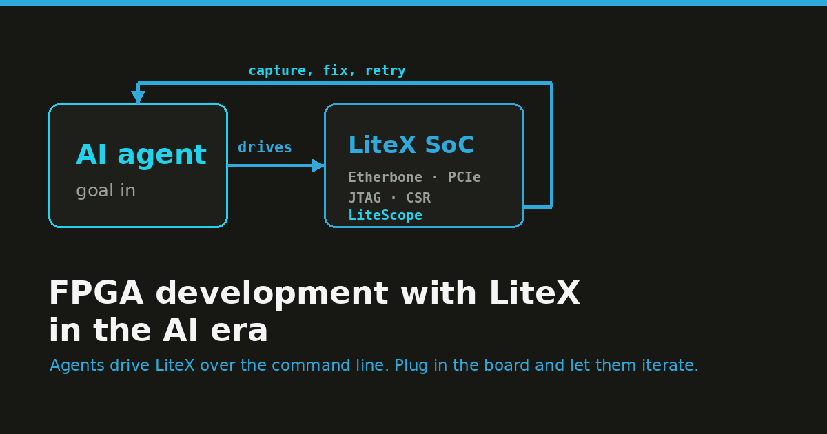
You can now put an FPGA board on the bench, give an agent a goal, and let it work: write the HDL, build it, load it, test it on real hardware, watch the bus with a logic analyzer, fix what is broken, and go round again. That works because LiteX has always been command-line and text first. No big IDE, no click-through GUI, no proprietary project format. You describe an SoC in Python, build it from the shell, and talk to the board with small command-line tools.
That was a deliberate, slightly boring choice, made for cost reasons. The goal at Enjoy-Digital was cost-effective hardware for clients: reuse common work, avoid reinventing the same blocks, avoid sinking time into heavy tooling. Text and a terminal travel everywhere, script easily, and need no license.
What we did not see coming is how well that fits the AI era. An agent is, more or less, very good with text and very happy running commands, and LiteX hands it a whole FPGA workflow that is already text and commands. It turns out we had been building the perfect interface for an agent for years, for entirely different reasons. 🙂
Why LiteX fits an agent#
The reason it works is that every step of FPGA development in LiteX has a text-and-command form, and an agent can reach all of them:
- Build and load:
./target.py --build --load. One command from Python SoC to bitstream on the FPGA. - Etherbone over Ethernet:
litex_server --udp ...plusRemoteClientscripts. Etherbone tunnels the SoC’s internal bus over Ethernet, so you can read and write any CSR (control/status register) from a Python one-liner. - PCIe bridge and rescan:
litex_server --pcie ...and arescan.pyto re-enumerate the device after a reload, so a fresh bitstream comes back without a reboot. - JTAG and UART:
litex_term, crossover UART through LiteX, JTAG access to the same bus. - CSR read/write: the whole register map is named and reachable, by software, by name.
- LiteScope: an in-fabric logic analyzer you configure from Python and trigger with
litescope_cli, dumping a.vcdyou can read back. - Simulation:
pytestand Verilator, so a change can be checked before it ever touches hardware. (Co-simulation makes that loop faster still: see QEMU co-simulation in LiteX.)

None of this was built for AI. It was built so a human could work fast from a terminal.
The loop#
Once the tools are reachable, the workflow is a loop. You give the agent a high-level goal and a spec, you put the target board on the bench, and it goes:

The important part is the bottom of that loop. When the design does not behave, the agent does not just stare at it. It adds a status CSR or a counter, or it adds a narrow LiteScope probe, rebuilds, reloads, triggers a capture over the bridge, reads back the waveform, and forms the next hypothesis. It writes its own observability. Then, when the bug is understood, it locks the fix in with a regression test so it cannot come back. (If you want the checklist version of this loop, the LiteX-M2SDR debugging guide is it.)
This matters because most of that loop is waiting and small decisions. An FPGA build is minutes, sometimes the better part of an hour. A bring-up is dozens or hundreds of these cycles. Very little of it needs senior-engineer judgement at each step. It needs patience and care, which is exactly the part you want to hand off. An agent does not get bored, wander off for coffee, or quietly give up at iteration 60. 🙂
Example 1: LiteNVMe#
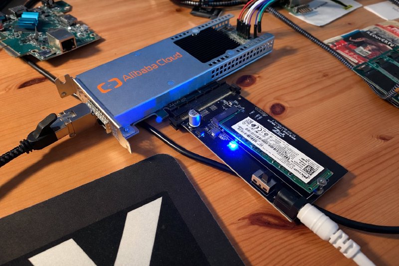
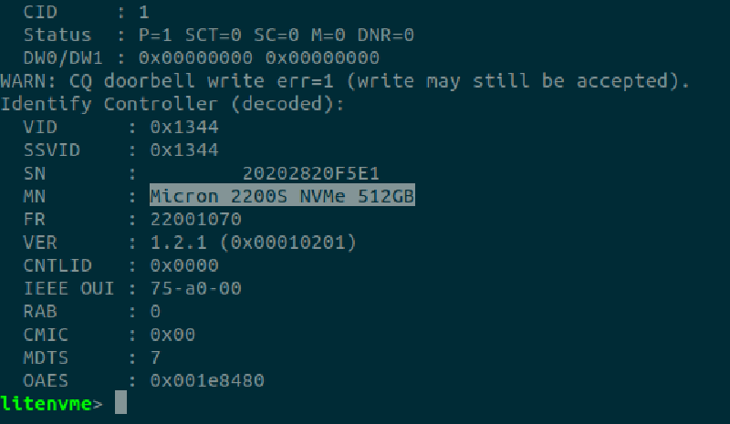
LiteNVMe is an open-source NVMe host core: the PCIe RootPort side that brings up an off-the-shelf SSD (enable the controller, Identify, create the I/O queues) and exposes a simple block interface, with no host CPU, OS or driver on the data path. Open-source NVMe host cores are rare, and this is the LiteX-native one. It is hardware-validated at PCIe Gen3 x4, about 2.7 GB/s.
The interesting thing for this post is not the core, it is the git history. With 284 commits, it reads like a lab notebook of exactly the loop above. A few real commit subjects:
bench: hostmem-write LiteScope probe + Gen3-256b HW harnesses & results
Lever B diagnosed: 128B MPS read ceiling is gateware-bound, not firmware-raisable
T6 coalescing on HW: functional (errors=0) but NO read speedup -- honest negative result
HONEST CORRECTION: pipelined-write fix was NEVER applied (dee81ba claim was false)
Read bottleneck fixed: pipelined hostmem write path ~2x reads on HW (~0.9-1.06 GB/s)
debug: nvme_mmiotest sets root bridge memory window; capture MMIO no-data completion
bench: prune one-off HW harnesses; factor shared boilerplate into hw_common.sh
You can see the whole method in there. Add a LiteScope probe to watch the host-memory write
path. Run a hardware harness, record the numbers. Diagnose a read ceiling and pin it to the
gateware rather than firmware. Try a coalescing change, measure it on hardware, and report an
honest negative result when it does not help. Catch a false claim and correct it (yes, that
HONEST CORRECTION commit is the agent fact-checking its own earlier commit, which is a genre
of git history I did not know I needed). And once a diagnostic probe has done its job, prune it
so it does not bloat the design. That last habit,
adding a probe to answer one question and then removing it, is the agent keeping its own
workspace clean.
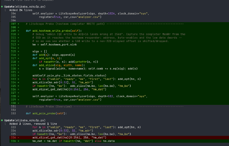
Here is one of those probes, written by the agent itself mid-debug. The comment is its own hypothesis (“does a 16-byte write to a non-32-byte-aligned offset get shifted or dropped at 256 bits?”), and the code wires up exactly the signals needed to answer it:
The end state is a real result: Gen3 x4, about 2.69 GB/s on 8 KiB reads and 2.74 GB/s on writes, errors zero, write then read-back bit-exact, on an Alibaba KU3P driving a commercial SSD. The remaining gap to the link ceiling is the SSD’s 512-byte MaxPayloadSize, not the core, which is itself something the loop figured out and wrote down.
Example 2: M2SDR, over the bridge#
The LiteX-M2SDR board (Artix-7 plus an AD9361
RFIC) is where we first wrote the methodology down and started testing it more extensively. Its
debugging guide
opens, literally, with “a practical starting point for developers or agents.” It is the loop
as a checklist: start from git status, reproduce on hardware, verify the host path with
m2sdr_util info, inspect the generated Verilog, add a CSR if polling can answer the question,
add a narrow LiteScope probe if the issue is temporal, capture, fix in the smallest layer, and
add a regression test. There is even a rule of thumb to keep captures under ~128 signal bits so
the build still closes timing.
That guide is really the team’s debugging instincts written down: the kind of skills a senior engineer carries in their head and applies without thinking. Which probe to reach for. When to drop the clock to 100 MHz before blaming the logic. Why a host write can pile up while the target quietly ignores it. As plain text, those skills stop being tacit. The agent reads them once and applies them on every run, instead of rediscovering the same workflow each time, and the guide itself improves as we learn new patterns. It is institutional knowledge that an agent can actually use.
The LiteSATA and Ethernet work on M2SDR is a good example of the unglamorous-but-necessary kind of iteration. Here is the Ethernet throughput, as it improved across the history that is recorded in the repo:
| Ethernet path | 8 MiB SigMF, host to SATA | SATA to host |
|---|---|---|
| Original Etherbone path | ~9.1 MiB/s | ~7.3 MiB/s |
| Pipelined Etherbone reads | ~9.1 MiB/s | ~26 MiB/s |
| 128 KiB SATA host buffer | ~47.8 MiB/s | ~25.5 MiB/s |
That is the shape of timing-and-throughput work: a long series of small changes, each measured on hardware, most of them boring, a few of them decisive. The same history also records the things that did not work and why, which is just as valuable:
- A 256 KiB host buffer was tried first and rejected because Vivado DRC failed on cascaded RAMB36 address pins. So the buffer is 128 KiB.
- An Etherbone burst-size sweep (1, 2, 4 … 128 words) showed where the throughput knee is.
- Linux
sendmmsg/recvmmsgbatching was tested and dropped: it landed within measurement noise, sometimes slower, so it was not kept.
Writing the dead ends down is the polite version of “stop suggesting this to me at 2am.”
A person can do all of that. But it is exactly the work where the value per decision is low and the number of iterations is high. It is the work you most want to delegate.
What this removes#
Put the two examples together and the pattern is clear. The expensive part of FPGA development is rarely the one clever idea. It is the long tail around it: waiting on builds, making small mechanical decisions, running the next iteration, reading back a capture, trying the next variant. The intelligence needed per step is low, but the steps are many (often well past a hundred for a real bring-up or a timing-closure campaign), and each one carries a multi-minute build.
That is precisely what an agent is good at now, because the FPGA loop is long and the agent is patient. You can let it run for hours, or across days, with only occasional guidance, and come back to a working prototype or a debugged design. Coming back to more progress than you left, instead of a stalled build and a cold coffee, takes some getting used to. The phase it eats into is the one where most of a project’s time actually goes: the early proof of concept and the debug grind, where you spend days chasing small details rather than designing anything.
With recent models (Claude Opus 4.8 and OpenAI GPT 5.5, both in high thinking) the guidance is needed less often than I expected. I mostly step in when the agent clearly loses the thread, and that is rarer than it used to be. More than once it has reached for a debug approach I would not have thought of. 🙂
The role this leaves me with is different, and honestly more pleasant. As a single developer I now work more like a project lead or an architect than someone typing every line: I decide what to build and why, set the architecture and the interfaces, write the spec, prepare the hardware, and review what comes back, while the agents handle the long mechanical middle. It also frees up time for things that are not engineering at all. Lately I have had more time to prepare the LiteX-M2SDR package and the hardware side of what we sell. 🙂
Where this goes#
The two examples are bring-up and throughput work, but the same loop covers a lot more, and this is the part I find most exciting to imagine:
- Early proof of concept. Give a spec and a board, get a first working prototype overnight, exactly the phase that usually eats weeks.
- Timing closure. Many iterations, low intelligence per step, long builds: change a directive or a pipeline, rebuild, read WNS/WHS (the worst-case timing slack), repeat. An agent can grind a hundred of these while you do something else.
- New-board bring-up. Point it at a new platform, let it work through clocking, resets and the first peripherals.
- Driver and software co-development. Bring the driver up against the gateware on real hardware, with the same CSR and capture access.
- Test farms. Several boards on the bench, an agent fanning regressions across all of them, bisecting a hardware regression to the commit that caused it.
- Porting cores across FPGA families, where most of the work is mechanical adaptation and re-validation.
- Exploration runs. Let it try variants of an architecture overnight and report back the ones that closed timing and passed, with the captures to prove it.
The common thread: in all of these, the human contribution is the goal, the spec, the hardware on the bench, and the occasional course-correction. The grind in between is now something you can hand off.
A caveat#
The split is the obvious one: the ideas and the engineering are mine, and I still steer when it matters. The agent runs the loop, not the project, and it runs it on real hardware with real captures and numbers.
It also only works because LiteX was text and commands from the start. A GUI-first tool could not be driven this way.
LiteNVMe: github.com/enjoy-digital/litenvme. LiteX-M2SDR: github.com/enjoy-digital/litex_m2sdr, and its debugging guide.
Work and ideas by Enjoy-Digital; written up with AI in the loop.